Color-tunable plasmonic device with a partially modulated refractive index

a plasmonic display and partially modulated technology, applied in the field of electronic visual display devices, can solve the problems of wasting the available light energy provided by the surroundings, requiring additional power to overcome the ambient light of the display, and display technologies all have disadvantages or challenges to overcome, so as to achieve the effect of reducing power consumption and fastness for video applications

Active Publication Date: 2011-10-25
SHARP KK
View PDF9 Cites 17 Cited by
  • Summary
  • Abstract
  • Description
  • Claims
  • Application Information

AI Technical Summary

Benefits of technology

[0010]Described herein is a method for the electrical tuning of the refractive index of the surrounding dielectric material. By making use of the tunable refractive index of liquid crystal or other electro-optical materials, the plasmonic resonance of the metal nanostructures can be tuned across the visible range and, thus, a pixel can exhibit different colors under different external voltages. Liquid crystal typically has a response time of a few milliseconds or shorter and, therefore, is fast enough for video applications. An extremely wide color tuning range, as well as a broad range of viewing angles has been unexpectedly achieved by using a tunable refractive index dielectric, in combination with a dielectric layer having a non-varying refractive index that at least partially surrounds a layer of plasmonic metal particles.
[0011]The color-tunable device operates with ambient light and does not normally require backlight illumination. The visual appearance of such a display may be like that of a traditional photograph, but with the capability to render both still and fast-moving images. Since ambient illumination is used to render these images, the power requirements of such a display are dramatically less than a standard LCD and, therefore, reduce the power consumption when introduced into devices such as a cellular phone or laptop. With this technology; the realization of video-embedded and interactive magazines and books is possible, the content of which can be modified electrically in real-time.

Problems solved by technology

Thus, the available light energy provided by these surroundings is wasted, and in fact, the operation of these displays requires additional power to overcome this ambient light.
These display technologies all have disadvantages or challenges that must be overcome to obtain greater commercial success.
Many existing technologies rely upon phenomena that are intrinsically slow.
Therefore, display techniques that rely on reactions to switch dye molecules demand unacceptably high currents for displaying video.
In particular, most reflective display technologies can only produce binary color (color / black) from one material set.
This limits the maximum reflected light for some colors to about ⅓, so that the pixel's of this type cannot produce saturated colors with a good contrast.
Finally, some reflective displays face reliability problem over a long lifetime.
Achieving the desired number of cycles is particularly difficult in reflective displays using techniques based on chemical reactions, techniques that involve mixing and separation of particles, or MEMS technology that involves repeated mechanic wear or electric stress.

Method used


Image

  • Color-tunable plasmonic device with a partially modulated refractive index
  • Color-tunable plasmonic device with a partially modulated refractive index
  • Color-tunable plasmonic device with a partially modulated refractive index

Examples


Embodiment Construction

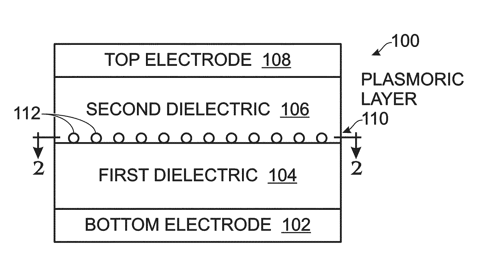
[0031]FIG. 1 is a partial cross-sectional view of a color-tunable plasmonic device with a partially modulated refractive index. The device 100 comprises an electrically conductive bottom electrode 102, and a first dielectric layer 104 overlying the bottom electrode 102. The first dielectric layer has a refractive index that is non-responsive to an electric field. Some examples of first dielectric materials include SiOx, SiNx, SiOxNy, MgF2, CaF2, SiOC, Teflon® AF, and organic polymers. However the device is not necessarily limited to just these materials. A second dielectric layer 106 overlies the first dielectric layer 104, having a refractive index responsive to an electric field. Some examples the second dielectric material include ferroelectric liquid crystals, nematic liquid crystals, LiNbO3, Hg2Cl2, LiTaO3, BBO, KTP, and organic electro-optical crystal 2,6-dibromo-N-methyl-4-nitroaniline. Again, the device 100 is not limited to just these materials. The change in refractive ind...


PUM

PropertyMeasurementUnit
sizeaaaaaaaaaa
refractive indexaaaaaaaaaa

Abstract

A color-tunable plasmonic device is provided with a partially modulated refractive index. A first dielectric layer overlies a bottom electrode, and has a refractive index non-responsive to an electric field. A second dielectric layer overlies the first dielectric layer, having a refractive index responsive to an electric field. An electrically conductive top electrode overlies the second dielectric layer. A plasmonic layer including a plurality of discrete plasmonic particles is interposed between the top and bottom electrodes. In one aspect, the plasmonic layer is interposed between the first and second dielectric layers. In a second aspect, the plasmonic layer is interposed between the first dielectric layer and the bottom electrode. In a third aspect, a first plasmonic layer is interposed between the first dielectric layer and the bottom electrode, and a second plasmonic layer of discrete plasmonic particles is interposed between the first dielectric layer and the second dielectric layer.

Description

BACKGROUND OF THE INVENTION[0001]1. Field of the Invention[0002]This invention generally relates to electronic visual display devices and, more particularly, to a color-tunable plasmonic display device that relies upon both modulated and non-modulated refractive index layers.[0003]2. Description of the Related Art[0004]Reflective display or color-tunable device technology is attractive primarily because it consumes substantially less power than liquid crystal displays (LCDs) and organic light emitting diode (OLED) displays. A typical LCD used in a laptop or cellular phone requires internal (backlight) illumination to render a color image. In most operating conditions the internal illumination that is required by these displays is in constant competition with the ambient light of the surrounding environment (e.g., sunlight or indoor overhead lighting). Thus, the available light energy provided by these surroundings is wasted, and in fact, the operation of these displays requires addi...

Claims


Application Information

Patent Timeline
Patent Type & Authority Patents(United States)
IPC IPC(8): G02F1/1335G02B26/00H01L21/00
CPCG02F1/19G02F1/23G02F2203/10G02F1/195
Inventor TANG, LIANGHASHIMURA, AKINORIVOUTSAS, APOSTOLOS T.
Owner SHARP KK
Why Eureka
Try Eureka