Group III nitride semiconductor light emitting device, method for producing the same, and lamp thereof

a technology of nitride semiconductors and light emitting devices, which is applied in the manufacture of semiconductor/solid-state devices, semiconductor devices, electrical devices, etc., can solve the problems of low thermal conductivity and achieve satisfactory crystallinity, excellent device characteristics, and low driving voltage

Active Publication Date: 2011-11-01
TOYODA GOSEI CO LTD
View PDF13 Cites 3 Cited by
  • Summary
  • Abstract
  • Description
  • Claims
  • Application Information

AI Technical Summary

Benefits of technology

[0040]The group III nitride semiconductor light emitting device of the present invention includes a semiconductor laminated structure, a light emitting layer, and electrodes each formed on the front surface and on the back surface of the semiconductor laminated structure, and in which the semiconductor laminated structure includes at least an impurity layer composed of a high concentration layer and a low concentration layer, and a group III nitride semiconductor layer, and the lower concentration layer and the high concentration layer are continuously formed on the group III nitride semiconductor layer in this order. Accordingly, it is possible to achieve a group III nitride semiconductor light emitting device having a double sided electrode structure and which has a low driving voltage as well as excellent device characteristics. More specifically, few pits and cracks are generated on the surface and satisfactory crystallinity is achieved when the low concentration layer is formed on the group III nitride semiconductor layer. In addition, the resistance of the impurity layer reduces resulting in the reduction of the resistance in the group III nitride semiconductor light emitting device when the high concentration layer is formed on the low concentration layer. Therefore, the semiconductor laminated structure having an impurity layer and in which a low concentration layer and a high concentration layer are continuously formed on a group III nitride semiconductor layer will have a low resistance as a whole and will also be excellent in terms of smoothness. Accordingly, the group III nitride semiconductor light emitting device of the present invention will have a low driving voltage as well as excellent light emission efficiency.
[0041]Moreover, in the group III nitride semiconductor light emitting device of the present invention, the low concentration layer is formed on the high concentration layer when a plurality of impurity layers are formed and each of which is arranged adjacent to one another. Accordingly, an advantageous effect is attained, that is, the pits and cracks formed in the high concentration layer will be filled by the low concentration layer. Therefore, the group III nitride semiconductor light emitting device will have an even more excellent semiconductor laminated structure in terms of smoothness.
[0042]In addition, according to the method for producing a group III nitride semiconductor light emitting device of the present invention, the low concentration layer and the high concentration layer are formed continuously on the group III nitride semiconductor layer in this order. Accordingly, due to the abovementioned effects of the low concentration layer to improve crystallinity and the high concentration layer to improve electrical conductivity, an impurity layer having a low resistance as a whole as well as excellent smoothness is formed, thereby achieving a group III nitride semiconductor light emitting device that has a low driving voltage as well as excellent light emission efficiency.
[0043]Moreover, since the lamp of the present invention is one that uses the group III nitride semiconductor light emitting device of the present invention, it will have a low driving voltage and excellent light emitting properties.

Problems solved by technology

Incidentally, since a sapphire substrate that is most widely used as a substrate constituting a group III nitride semiconductor light emitting device is an insulator and thus has a disadvantage of having low thermal conductivity, there is a demand for the development of substrates to serve as an alternative to the sapphire substrate.

Method used


Image

  • Group III nitride semiconductor light emitting device, method for producing the same, and lamp thereof
  • Group III nitride semiconductor light emitting device, method for producing the same, and lamp thereof
  • Group III nitride semiconductor light emitting device, method for producing the same, and lamp thereof

Examples


example 1

[0094]A base 1 which was a Si (111) substrate was prepared. An n-type group III nitride semiconductor layer 2 made of Si-doped GaN was formed on the base 1 by a vacuum MBE method via a buffer layer made of AlN to obtain a substrate 20.

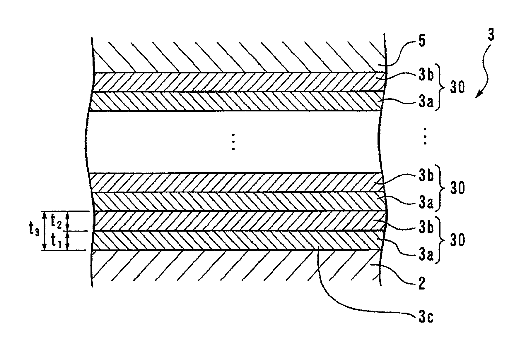
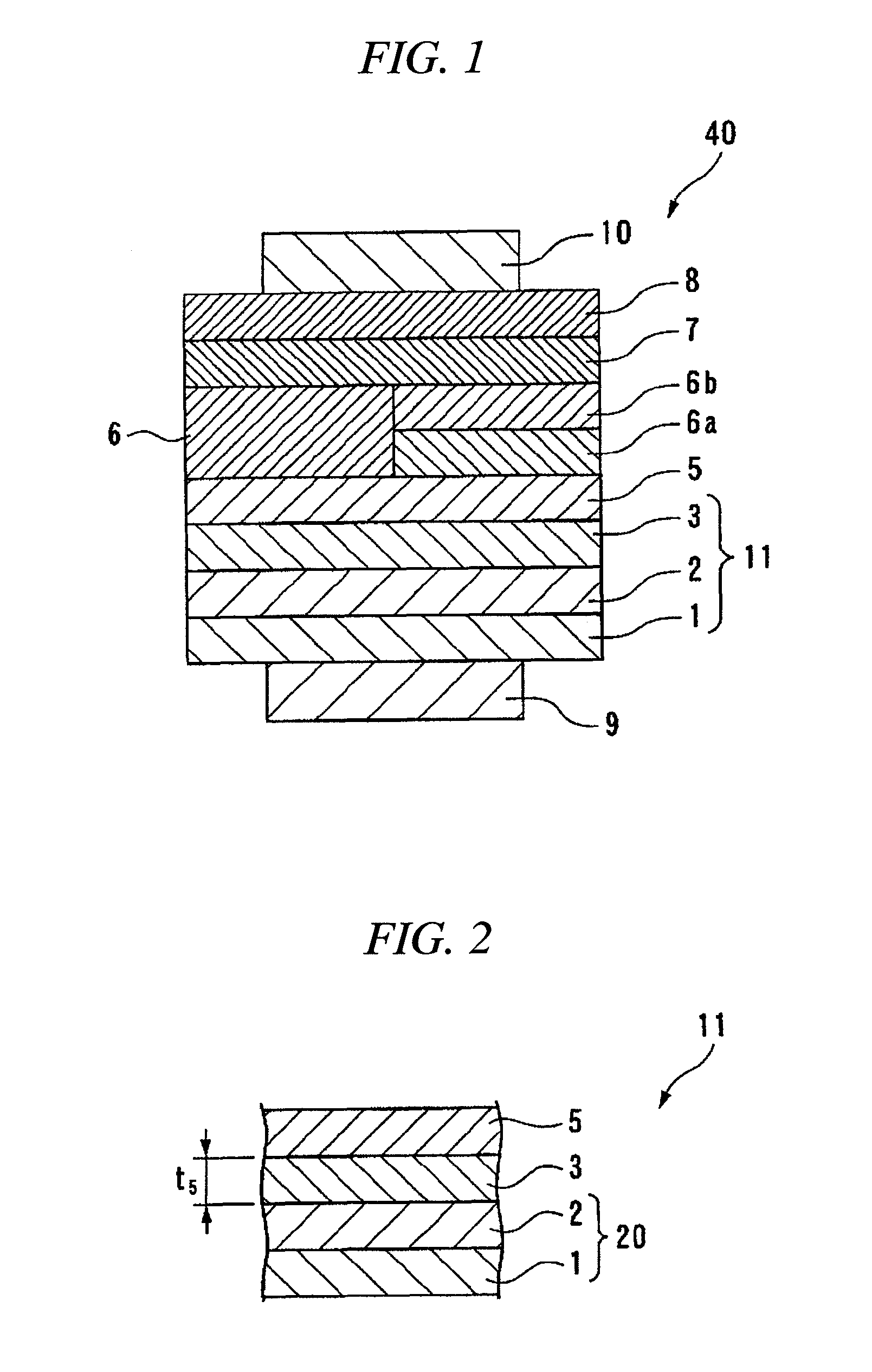
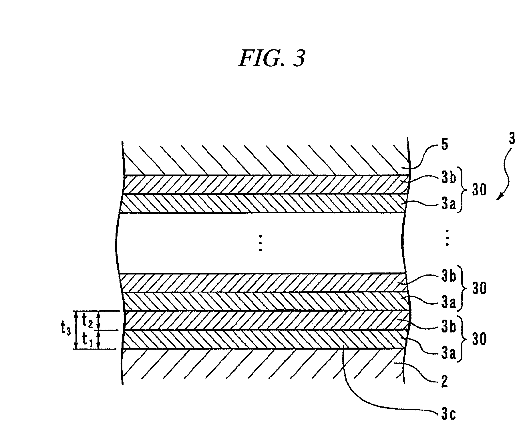
[0095]Subsequently, the repetitive impurity layer shown in FIG. 3 was formed on the group III nitride semiconductor layer 2 of the substrate 20, as described below, to obtain a semiconductor laminated structure 11 shown in FIG. 2.

[0096]To form the repetitive impurity layer 3, the substrate 20 was first introduced in an MOCVD apparatus and was mounted on a susceptor made of highly pure graphite for semiconductors which was heated to a film forming temperature by a radiofrequency (RF) induction heater. Thereafter, nitrogen gas was circulated in a vapor phase growth reaction furnace made of stainless steel for purging inside the furnace.

[0097]After circulating the nitrogen gas in the vapor phase growth reaction furnace for 8 minutes, the induction heater ...


PUM


Abstract

A group III nitride semiconductor light emitting device with a double sided electrode structure which has a low driving voltage as well as excellent light emission efficiency is provided, and the group III nitride semiconductor light emitting device includes at least an impurity layer 30 composed of a high concentration layer 3b made of a group III nitride semiconductor containing high concentration of impurity atoms, and a low concentration layer 3a made of a group III nitride semiconductor containing impurity atoms whose concentration is lower than that of the high concentration layer 3b; and a group III nitride semiconductor layer 2, and the lower concentration layer 3a and the high concentration layer 3b are continuously formed on the group III nitride semiconductor layer 2 in this order to form the group III nitride semiconductor light emitting device.

Description

TECHNICAL FIELD[0001]The present invention relates to a group III nitride semiconductor light emitting device, a method for producing the same, and a lamp thereof. In particular, the present invention relates to a group III nitride semiconductor light emitting device that employs a semiconductor laminated structure having low resistance, excellent smoothness, a low driving voltage, and excellent device characteristics.[0002]Priority is claimed on Japanese Patent Application No. 2006-082473, filed Mar. 24, 2006, the content of which is incorporated herein by reference.BACKGROUND ART[0003]A group III nitride semiconductor formed on a substrate has been used conventionally as a functional material for constituting a group III nitride semiconductor light emitting device having a pn junction structure such as a light emitting diode (LED) and a laser diode (LD) that irradiate short wavelength visible light (for example, refer to Patent Document 1). For example, in the LED emitting near ul...

Claims


Application Information

Patent Timeline
Patent Type & Authority Patents(United States)
IPC IPC(8): H01L33/00H01L33/32H01L33/06H01L33/54H01L33/56H01L33/60H01L33/62
CPCH01L33/025H01L33/007H01L33/02H01L21/02381H01L21/02458H01L21/02507H01L21/0254H01L21/0262H01L33/04H01L21/02573H01L2224/48091H01L2224/73265H01L2224/45144H01L2924/00014H01L2924/00
Inventor MIKI, HISAYUKISAKAI, HIROMITSU
Owner TOYODA GOSEI CO LTD
Why Eureka
Try Eureka