Semiconductor device

a technology of semiconductors and devices, applied in the field of semiconductor devices, can solve the problems of inability to set the resistance value of the reference resistance more appropriately according to the resistance distribution, and inability to read information from more than an allowable number of memory cells

Inactive Publication Date: 2012-01-10
LONGITUDE LICENSING LTD
View PDF6 Cites 53 Cited by
  • Summary
  • Abstract
  • Description
  • Claims
  • Application Information

AI Technical Summary

Benefits of technology

[0013]This invention makes it possible to measure the resistance distribution of a plurality of memory cells, and thus to set the reference level more appropriately according to the resistance distribution obtained by the measurement.

Problems solved by technology

In the case of a semiconductor device having a single reference resistance element for a plurality of memory cells, it may be impossible to read information from more than an allowable number of memory cells depending on characteristics of the memory cells.
However, I have now discovered that Patent Document 1 does not describe at all how to set a reference potential when there are a large number of memory cells and there is resistance distribution.
Consequently, the semiconductor device described in Patent Document 1 has a drawback that it is impossible to set the resistance value of the reference resistance more appropriately when there is resistance distribution among a plurality of memory cells.
Consequently, this semiconductor device also has a drawback, similarly to the one described in Patent Document 1, that it is impossible to set the resistance value of the reference resistance more appropriately according to the resistance distribution.

Method used


Image

  • Semiconductor device
  • Semiconductor device
  • Semiconductor device

Examples


first embodiment

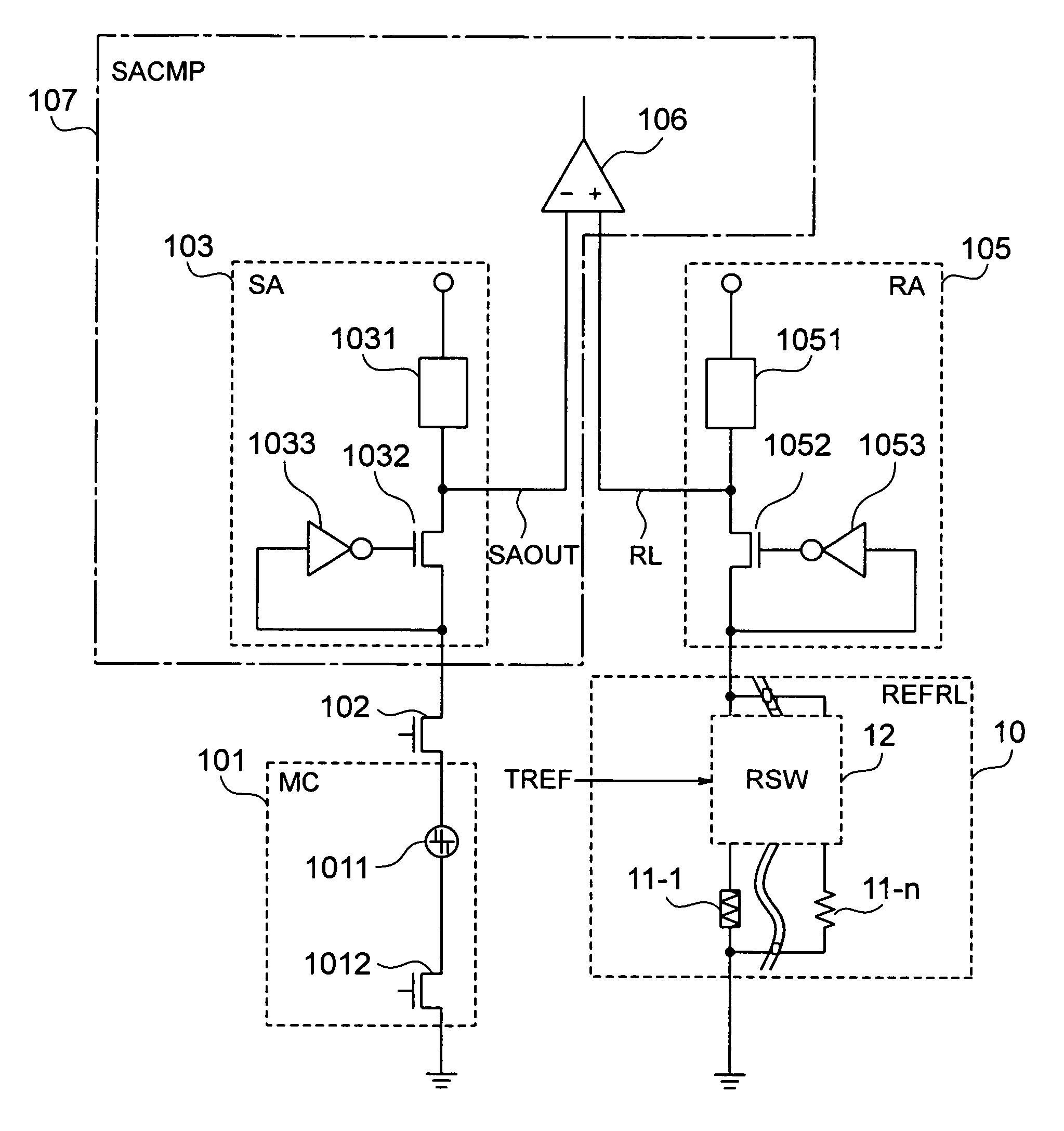
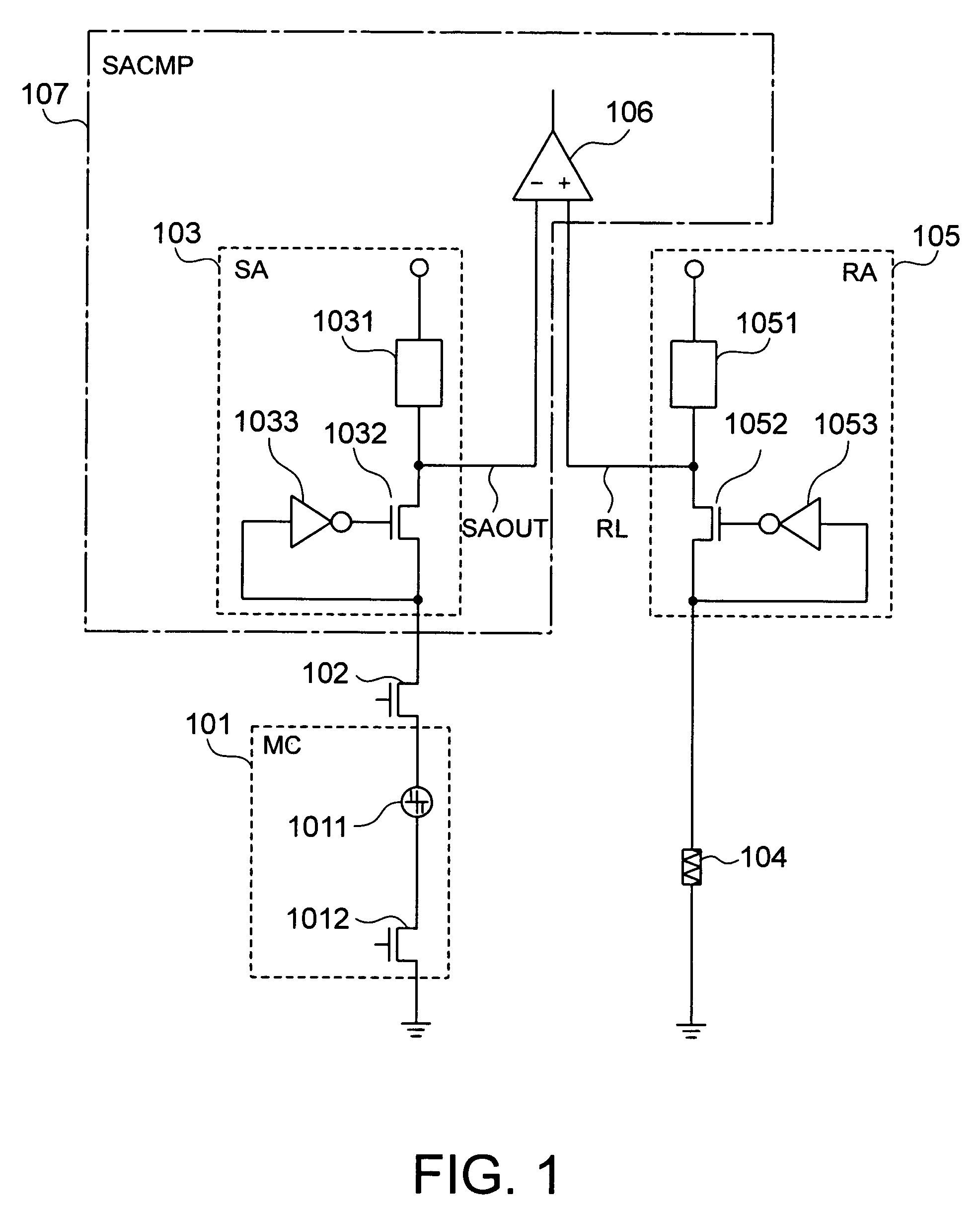
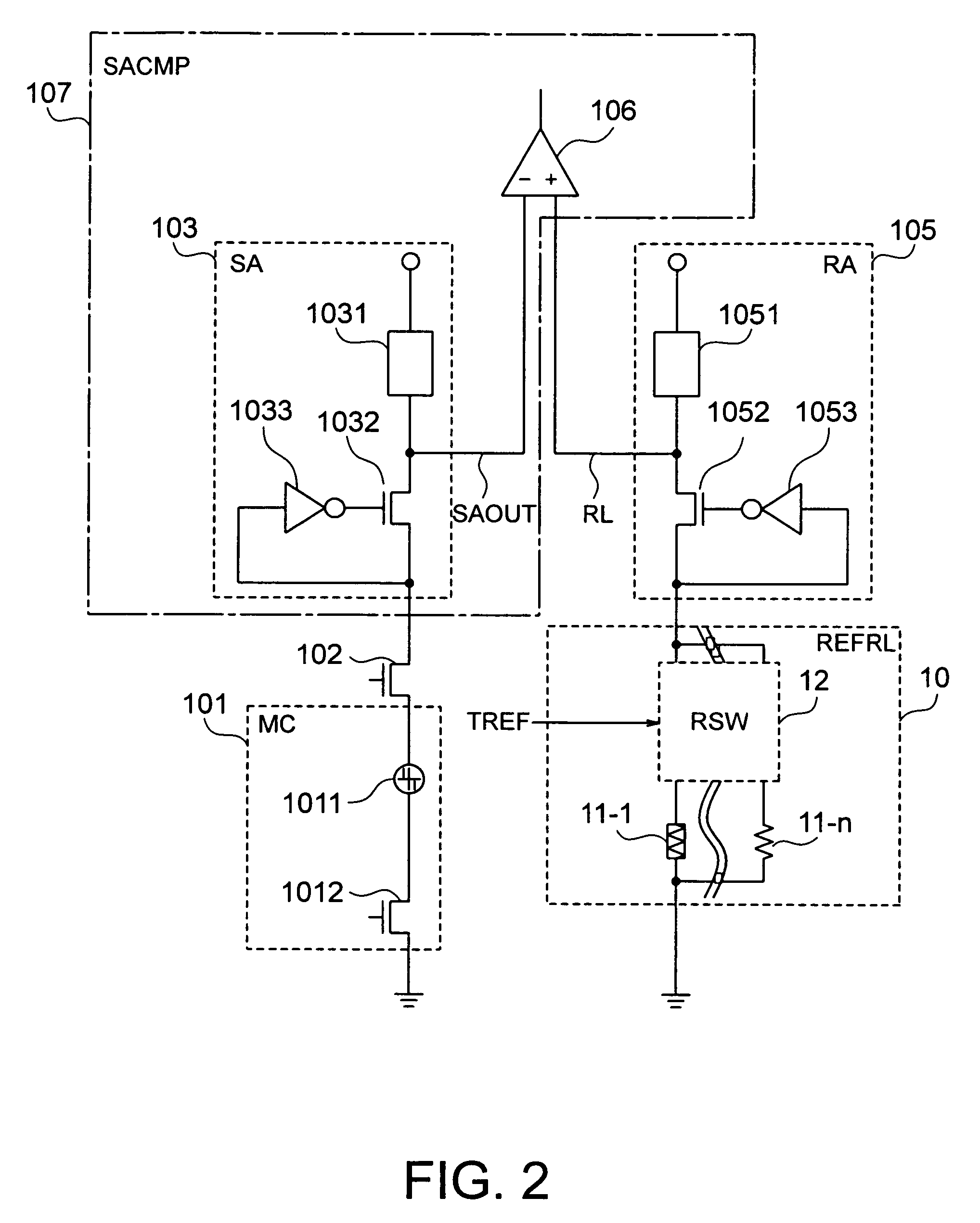
[0037]FIG. 2 shows a configuration of a principal part of a semiconductor device according to this invention. In FIG. 2, like components as those of the related semiconductor device shown in FIG. 1 are assigned with the same reference numerals, and description thereof will be omitted. It should be understood that although only one memory cell 101 is shown in FIG. 2, a plurality of memory cells are connected in common (in a hierarchical manner) to the sense amplifier 103 via the respective Y switches.

[0038]The semiconductor device shown in FIG. 2 has a reference system circuit (REFRL) 10 in place of the conventional referential resistance element 104.

[0039]The reference system circuit 10 has n (n is a natural number) referential resistances (RREF1 to RREFn) 11-1 to 11-n one end of each of which is grounded, and a resistance selection circuit (RSW) 12 connected to the other ends of these referential resistances. The resistance selection circuit 12 selectively connects at least one of ...

second embodiment

[0061]Next, this invention will be described with reference to FIG. 10.

[0062]Whereas fuses are provided in the reference level decoder RLDEC in the first embodiment, fuses are provided within a reference system circuit 90 in this second embodiment. This eliminates the need of the reference level decoder RLDEC in the second embodiment.

[0063]Describing in more detail, the reference system circuit 90 has a plurality of referential resistance elements 91-1 to 91-n (n referential resistance elements in this example) one ends of which are grounded. The resistance values of the referential resistance elements 91-1 to 91-n are different from one another, for example. The other ends of the referential resistance elements 91-1 to 91-n are connected to one ends of fuses 92-1 to 92-n, respectively. The other ends of the fuses 92-1 to 92-n are connected to one ends of reference resistance selector switches 93-1 to 93-n, respectively. The other ends of the reference resistance selector switches 9...


PUM


Abstract

A semiconductor device has a plurality of memory cells including memory elements to store information by varying resistance values of the memory elements. The semiconductor device further has a reference system circuit enables measurement of distribution of the resistance values for the plurality of memory cells.

Description

[0001]This application is based upon and claims the benefit of priority from Japanese patent application No. 2008-142098, filed on May 30, 2008, the disclosure of which is incorporated herein in its entirety by reference.BACKGROUND OF THE INVENTION[0002]1. Field of the Invention[0003]This invention relates to a semiconductor device and, in particular, to a semiconductor device having resistance variable memory cells.[0004]2. Description of the Related Art[0005]A resistance variable memory cell includes a memory element for storing information as variation in resistance. A voltage at a predetermined level is applied to a memory element serially connected to a load with a predetermined resistance, whereby an output voltage corresponding to the resistance of the memory element can be obtained at a node between the memory element and the load. Information written in the memory element is read out by comparing this output voltage with a reference voltage.[0006]The reference voltage is ob...

Claims


Application Information

Patent Timeline
Patent Type & Authority Patents(United States)
IPC IPC(8): G11C11/00
CPCG11C13/0004G11C29/52G11C29/50008G11C29/50
Inventor TONOMURA, YASUKO
Owner LONGITUDE LICENSING LTD
Why Eureka
Try Eureka