Display device, electronic device, and method of driving display device

a technology of display device and electronic device, which is applied in the direction of electric digital data processing, instruments, computing, etc., can solve the problems of reliability degradation and acceleration of temporal reduction of emission current value, and achieve the suppression of the acceleration of temporal reduction of light emission current value, prolonging the write time, and suppressing the vth of the first transistor

Active Publication Date: 2012-01-17
JOLED INC
View PDF4 Cites 5 Cited by
  • Summary
  • Abstract
  • Description
  • Claims
  • Application Information

AI Technical Summary

Benefits of technology

[0013]In view of foregoing, it is desirable to provide a display device and an electronic device, of which the reliability may be improved compared with the related art, and a method of driving the display device.
[0018]In the display device, the electronic device, and the method of driving the display device of an embodiment of the invention, the control signal instructs the first drive section to establish ON-period of the first transistor within a period in which voltage of the second wiring is maintained to the third voltage to set the photo-emission element into an extinction state and voltage of the third wiring is maintained to the fifth voltage, the ON-period of the first transistor being defined as a period from a timing at which voltage of the first wiring rises from the first voltage to the second voltage to another timing at which the voltage of the first wiring falls from the second voltage to the first voltage. This accelerates plus shift (variation in a positive voltage direction) of Vth (threshold voltage) of the first transistor, enabling cancel of a variation level of minus shift (variation in a negative voltage direction) of Vth (threshold voltage) of the first transistor in the past. Therefore, variation in Vth of the first transistor is suppressed, which suppresses acceleration in temporal reduction in light emission current value due to lengthened write time caused by such variation in Vth.
[0019]According to the display device, the electronic device, and the method of driving the display device of an embodiment of the invention, the control signal instructs the first drive section to establish ON-period of the first transistor within a period in which voltage of the second wiring is maintained to the third voltage to set the photo-emission element into an extinction state and voltage of the third wiring is maintained to the fifth voltage, the ON-period of the first transistor being defined as a period from a timing at which voltage of the first wiring rises from the first voltage to the second voltage to another timing at which the voltage of the first wiring falls from the second voltage to the first voltage. Therefore variation in Vth of the first transistor is suppressed, and consequently acceleration in temporal reduction in light emission current value may be suppressed. Accordingly, reliability may be improved compared with the related art.

Problems solved by technology

This results in a difficulty that temporal reduction in emission current value is accelerated due to such lengthened write time.
In this way, in the related art, temporal reduction in emission current value is disadvantageously accelerated due to lengthened write time caused by variation in Vth of the sampling transistor, leading to reliability degradation, and there is a room for improvement.

Method used


Image

  • Display device, electronic device, and method of driving display device
  • Display device, electronic device, and method of driving display device
  • Display device, electronic device, and method of driving display device

Examples


application examples

MODULE AND APPLICATION EXAMPLES

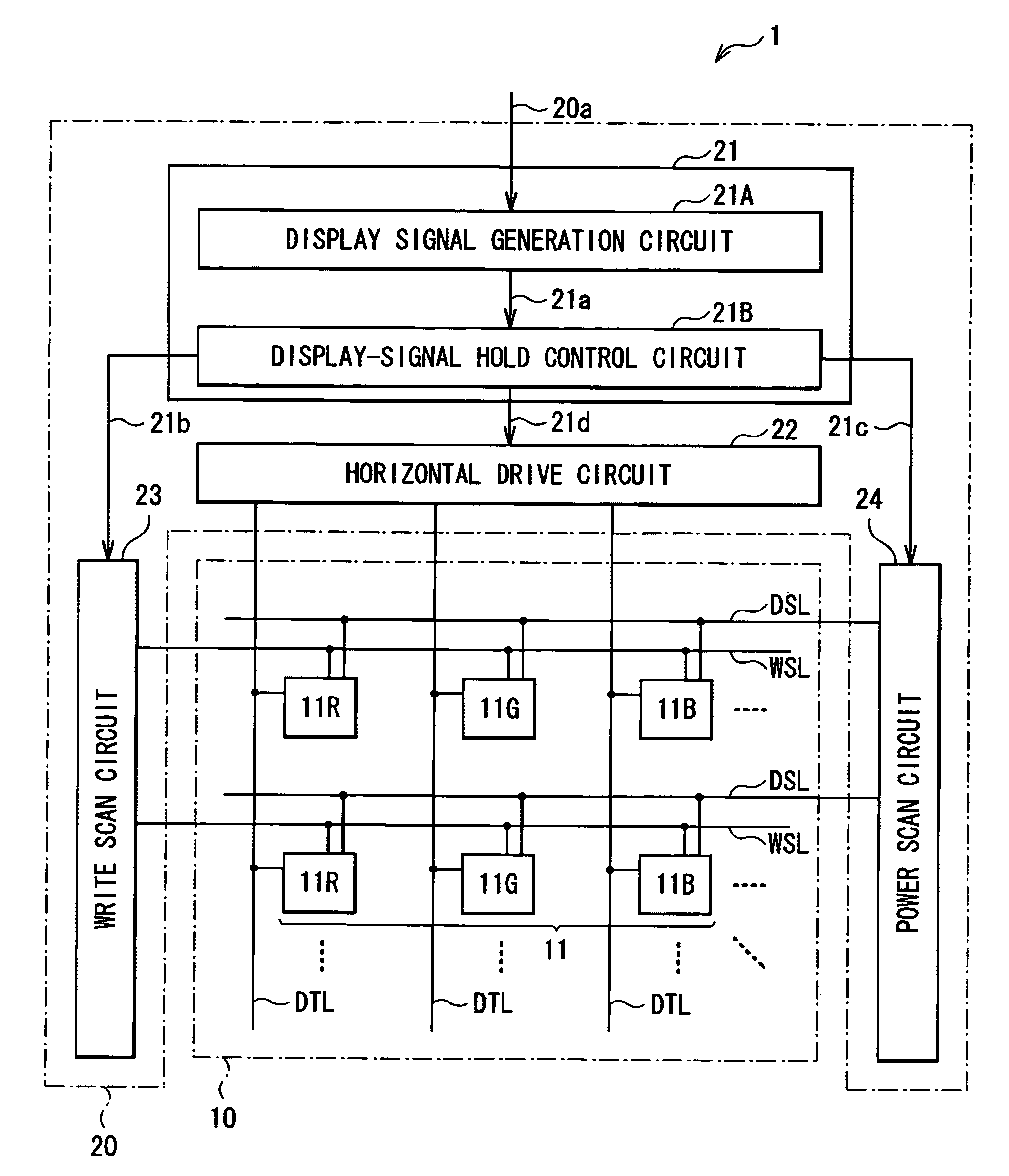
[0086]Hereinafter, description is made on application examples of the display device 1 described in the embodiment. The display device 1 of the embodiment may be applied to an electronic device in any filed, including a television device, a digital camera, a notebook personal computer, a mobile terminal device such as mobile phone, or a video camera. In other words, the display device 1 of the embodiment may be applied to a display device of an electronic device in any filed, the display device displaying an externally inputted video signal or an internally produced video signal in a form of a still or moving image.

[0087]Module

[0088]The display device 1 of the embodiment is incorporated in various electronic devices such as application examples 1 to 5 described later, for example, in a form of a module as shown in FIG. 12. The module has, for example, a region 210 exposed from a member (not shown) sealing the display section 10 on one side of the subst...

application example 1

[0089]FIG. 13 shows appearance of a television device using the display device 1 of the embodiment. The television device has, for example, a video display screen section 300 including a front panel 310 and a filter glass 320, and the section 300 includes the display device 1 according to the embodiment.

application example 2

[0090]FIGS. 14A and 14B show appearance of a digital camera using the display device 1 of the embodiment. The digital camera has, for example, a flash light emission section 410, a display section 420, a menu switch 430, and a shutter button 440, and the display section 420 includes the display device 1 according to the embodiment.


PUM


Abstract

A display device is provided having improved reliability compared with the related art. The display device includes, for each pixel: a photo-emission element and a first MOS transistor connected in series between a first power source line and a second power source line; a capacitor connected to be inserted between a gate and a source of the first MOS transistor; and a second MOS transistor connected to be inserted between a signal line to be applied with a image signal voltage and the gate of the first MOS transistor, the second MOS transistor being controlled by a scan signal to change between ON-state and OFF-state, wherein ON-period of the first transistor is established within a period in which the photo-emission element is maintained to an extinction state and the signal line is applied with a voltage having a fixed level independent from the image signal voltage.

Description

BACKGROUND OF THE INVENTION[0001]1. Field of the Invention[0002]The present invention relates to a display device including a display section having a photo emission element and a pixel circuit for each pixel, and a method of driving the display device, and to an electronic device having such a display device.[0003]2. Description of the Related Art[0004]Recently, in a field of a display device performing image display, a display device is developed and progressively commercialized, which uses a current-drive optical element, for example, an organic EL (Electro Luminescence) element, as a photo emission element of a pixel, emission luminance of the optical element varying depending on a current value.[0005]The organic EL element is a self-luminous element unlike a liquid crystal element. Therefore, a display device using the organic EL element (organic EL display device) does not need a light source (backlight), and therefore the display device is high in visibility of an image, low ...

Claims


Application Information

Patent Timeline
Patent Type & Authority Patents(United States)
IPC IPC(8): G09G5/00
CPCG09G3/3233G09G3/3258G09G2300/0819G09G2310/06G09G2300/0866G09G3/30G09G3/20
Inventor TOYOMURA, NAOBUMIUCHINO, KATSUHIDE
Owner JOLED INC
Why Eureka
Try Eureka