III-V photonic integration on silicon

a technology of photonic integration and silicon, applied in the field of semiconductor devices, can solve the problems of difficult growth on silicon, difficult integration with electronic devices manufactured on silicon, cost and size are much smaller,

Active Publication Date: 2012-02-07
RGT UNIV OF CALIFORNIA
View PDF7 Cites 71 Cited by
  • Summary
  • Abstract
  • Description
  • Claims
  • Application Information

AI Technical Summary

Benefits of technology

[0010]To minimize the limitations in the prior art, and to minimize other limitations that will become apparent upon reading and understanding the present specification, the present invention provides a technology for making photonic integrated circuits on silicon. By bonding a wafer of III-V material as an active region to silicon and removing the substrate, the lasers, amplifiers, modulators, and other devices can be processed using standard photolithographic techniques on the silicon substrate. The coupling between the silicon waveguide and the III-V gain region allows for integration of low threshold lasers, tunable lasers, and other photonic devices and integrated circuits with Complimentary Metal Oxide Semiconductor (CMOS) integrated circuits.

Problems solved by technology

These devices are difficult to integrate with electronic devices fabricated on silicon.
However, most active photonic devices require single crystal material, which is difficult to grow on silicon because of the large lattice mismatch between the semiconductor with the proper bandgaps and silicon itself.
The problem with the present discrete photonic devices is that the performance can be improved with integration, and the cost and size is much smaller.
However, silicon-based modulators or lasers or other photonic devices are not as efficient at light emission or absorption as their III-V based counterparts.

Method used


Image

  • III-V photonic integration on silicon
  • III-V photonic integration on silicon
  • III-V photonic integration on silicon

Examples


Embodiment Construction

[0028]In the following description, reference is made to the accompanying drawings which form a part hereof, and which is shown, by way of illustration, several embodiments of the present invention. It is understood that other embodiments may be utilized and structural changes may be made without departing from the scope of the present invention.

Overview

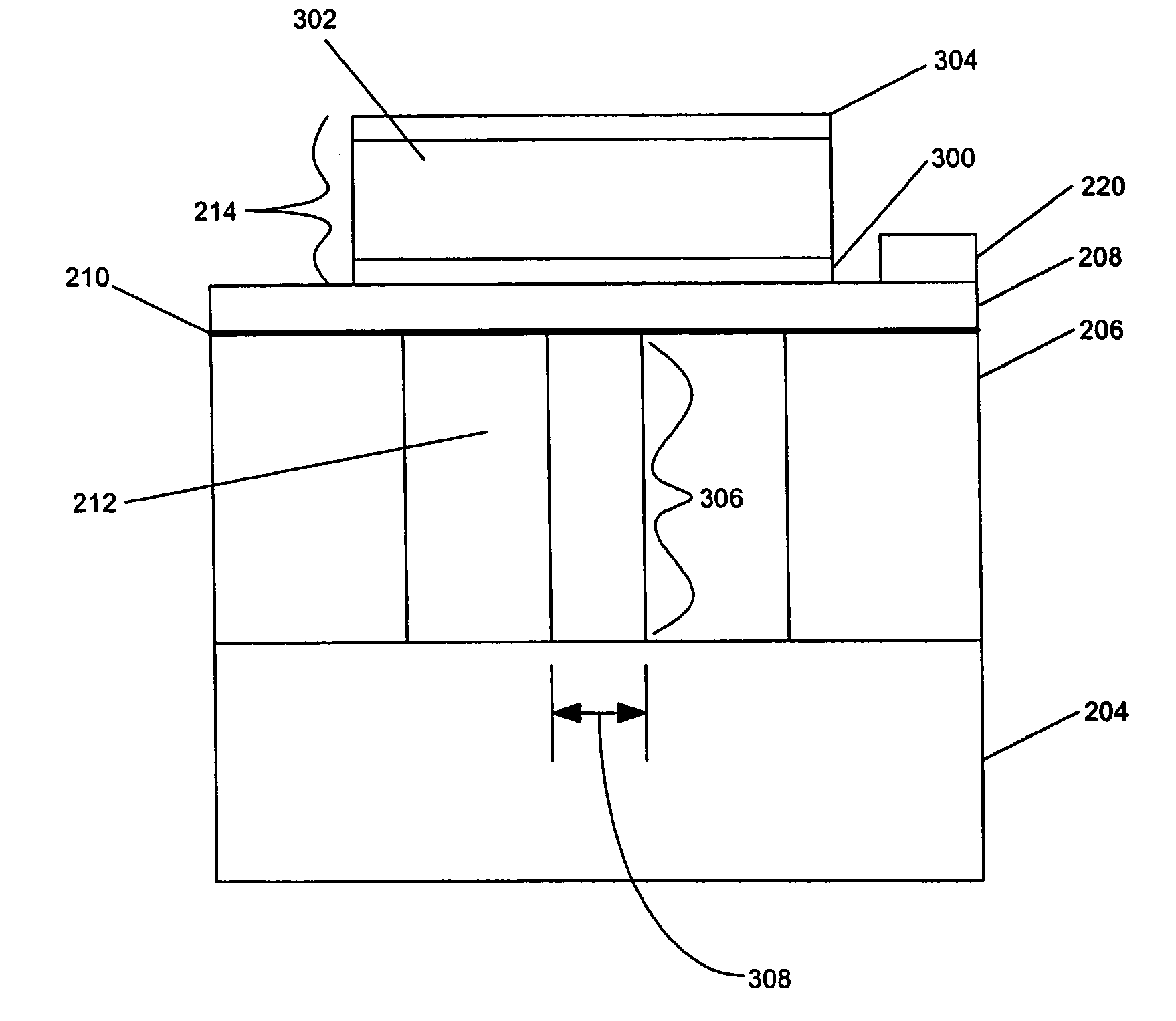
[0029]FIG. 1 is a side view of a photonic integrated circuit in accordance with the present invention.

[0030]Device 100 is shown, with wafer 102, film 103, waveguide layer 104, modulator / mode converter 106, gain region 108, and photodetector 110 as shown. DBR reflector 112 are also shown.

[0031]Wafer 102 is typically a silicon CMOS wafer, but can be other materials, such as glass, as desired. Film 103 is typically silicon oxide, but can also be a nitride or silicon oxynitride if desired without departing from the scope of the present invention. Waveguide layer 104 is on film 103, and is the silicon waveguide layer for device 100. Modul...


PUM


Abstract

Photonic integrated circuits on silicon are disclosed. By bonding a wafer of III-V material as an active region to silicon and removing the substrate, the lasers, amplifiers, modulators, and other devices can be processed using standard photolithographic techniques on the silicon substrate. The coupling between the silicon waveguide and the III-V gain region allows for integration of low threshold lasers, tunable lasers, and other photonic integrated circuits with Complimentary Metal Oxide Semiconductor (CMOS) integrated circuits.

Description

CROSS-REFERENCE TO RELATED APPLICATIONS[0001]This application claims the benefit under 35 U.S.C. Section 119(e) of the following co-pending and commonly-assigned U.S. provisional patent applications:[0002]Ser. No. 60 / 760,629, filed Jan. 20, 2006, entitled “OPTICAL GAIN AND LASING ON SILICON,” by John E. Bowers, and[0003]Ser. No. 60 / 795,064, filed Apr. 26, 2006, entitled “III-V PHOTONIC INTEGRATION ON SILICON,” by John E. Bowers,[0004]which applications are incorporated by reference herein.BACKGROUND OF THE INVENTION[0005]1. Field of the Invention[0006]The present invention relates generally to semiconductor devices, and, more specifically, to integration of III-V optical devices with silicon substrates and circuits.[0007]2. Description of the Related Art[0008]Semiconductor chip level bonded devices have found uses in several consumer and commercial applications. Typically, semiconductor devices are made from a single type of material, or different types of material are grown onto a ...

Claims


Application Information

Patent Timeline
Patent Type & Authority Patents(United States)
IPC IPC(8): H01L29/06
CPCH01L31/1852H01S5/021H01S5/0268H01S5/125H01S5/0208G02F1/01708H01S5/343G02B6/1225G02B6/12002H01S5/0261H01S5/0215H01L27/146G02B2006/12107H01S5/0217H01S5/18341H01S5/18369Y02E10/544G02B2006/12147G02B2006/12128G02B2006/12121G02B2006/12061H01L31/125Y02P70/50
Inventor BOWERS, JOHN E.
Owner RGT UNIV OF CALIFORNIA
Why Eureka
Try Eureka