Fabrication process of a trench gate power MOS transistor with scaled channel

a technology of power mos transistor and fabrication process, which is applied in the direction of electrical equipment, instruments, static storage, etc., can solve the problems of limited level of performance that can be achieved, limited scale down of lateral dimensions (and packing), and limited design and fabrication of power vdmos transistors with scaled dimensions but with high current capabilities. , to achieve the effect of reducing the resistance of the gate electrode, and less electrical resistivity

Inactive Publication Date: 2005-05-03
STMICROELECTRONICS SRL
View PDF5 Cites 24 Cited by
  • Summary
  • Abstract
  • Description
  • Claims
  • Application Information

AI Technical Summary

Benefits of technology

[0006]In view of the foregoing background, an object of the present invention is to form a power MOS device with a trench in the active area but with geometries of the polysilicon gate, body, source and contacts being self-aligned to the trench so that a low cost submicron elementary MOS structure is formed without requiring the formation of any initial spacer. This minimizes limitations resulting from the reduction of lateral dimensions when using an initial spacer. The advantages typically associated with an active trench structure include the elimination of the JFET contribution to the ON-resistance, and the reduction of accumulations and epitaxy contributions thereto.
[0007]According to the invention, a MOS transistor with a trench gate is formed with a process that allows self-alignment of the polysilicon gate structure to the trench itself, and the successive self-alignment of the body and source implantations to the polysilicon window itself. In this way, the critical steps associated with carrying out the photolithographic masking steps for defining submicron features, such as the polysilicon gate and body implantations, are avoided.
[0009]According to yet a further embodiment, the body / source short-circuiting contact in the active area may be realized using a further submicron trench in the diffused silicon, with a depth greater than the depth of the source diffusion. In this way, it is possible to eliminate the photolithographic masking step for defining the source.
[0015]The filling oxide forms the hard mask for defining the self-aligned polysilicon gate during the anisotropic (vertical) etching of the polysilicon. An evident advantage of the structure realized with the method of the invention results in a net reduction in the defects of the fabrication process because of the elimination of relatively critical masking steps. The reduction of fabrication costs that are achieved is also evident.
[0018]According to a further embodiment, a deposition on or growth of a silicide layer at the surface of the deposited layer of polysilicon may be carried out for forming a stack having less electrical resistivity than that of the polysilicon layer having the same thickness. This is done to reduce the resistance of the gate electrode patterned from such a stack. This may be useful or necessary because the relatively small thickness of the polysilicon layer deposited in the trench may represent an intrinsic limit to the conductivity of the patterned gate electrode, and as a consequence, to the switching speed of the device. Appropriately enhanced layout approaches (distribution of the gates in the active area) may be implemented for reducing the gate electrode resistance without necessarily coupling a metal silicide film onto the deposited polysilicon layer.

Problems solved by technology

Designing and fabricating power VDMOS transistors having scaled dimensions but with high current capabilities is limited with respect to nested geometries being formed within an elementary unit in an active area.
Moreover, even if it were possible to accurately align structures in submicron spaces, certain contributions to the ON-resistance of the integrated device would still limit the level of performance that can be achieved.
This is a complicated process, and introduces a limitation in the scaling down of lateral dimensions (and to the packing) as a consequence of using an initial spacer.

Method used


Image

  • Fabrication process of a trench gate power MOS transistor with scaled channel
  • Fabrication process of a trench gate power MOS transistor with scaled channel
  • Fabrication process of a trench gate power MOS transistor with scaled channel

Examples


first embodiment (

Epitaxial Body):

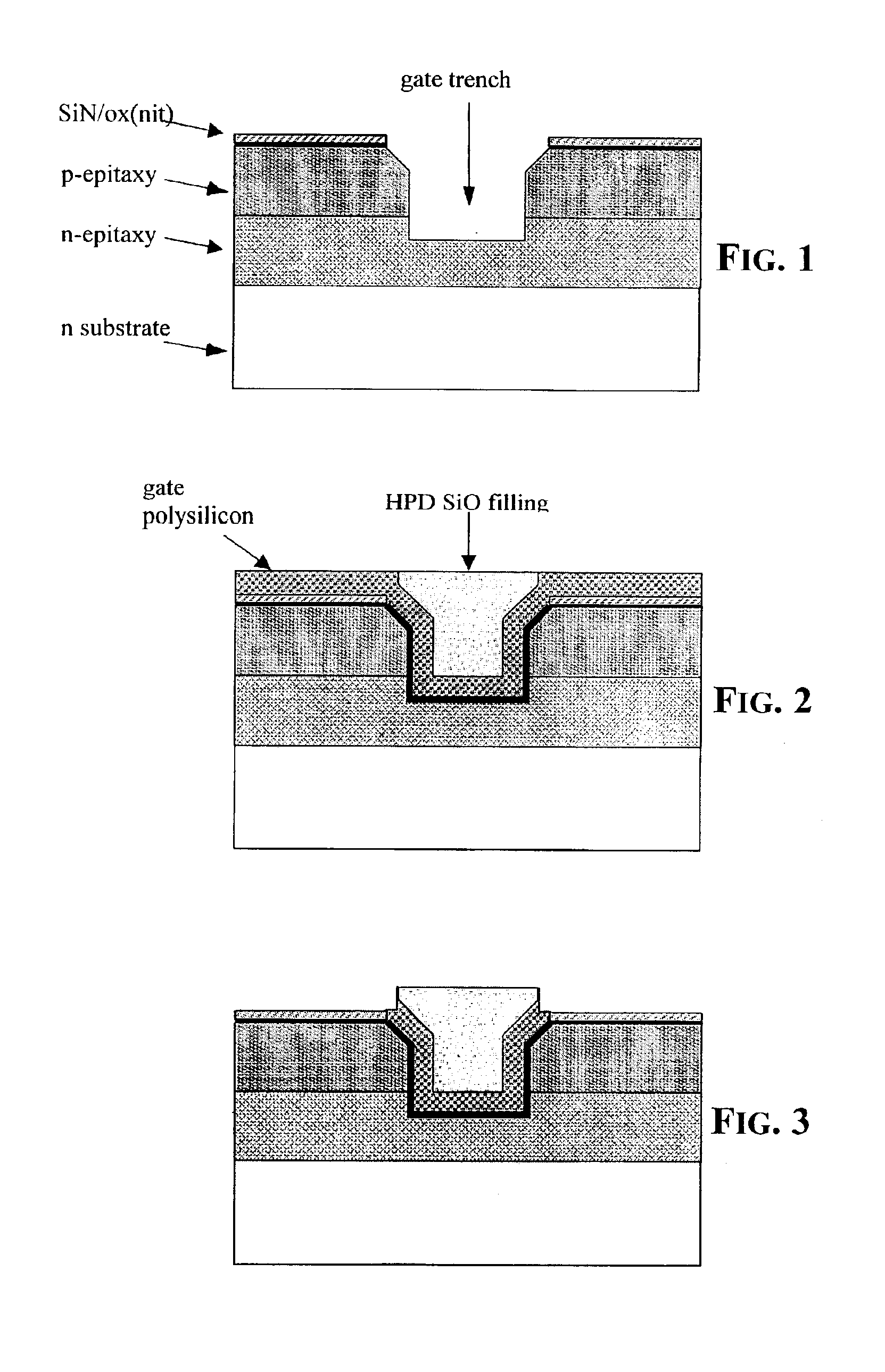
[0023]A double epitaxial layer is formed: substrate (n+) / epi-Si (n) / epi-Si (p) (body). The edge structure and the active area are defined according to any one of the prior art techniques. The second epitaxial layer will have the desired type of conductivity for the body region of the transistor, opposite to the type of conductivity of the first epitaxial layer.

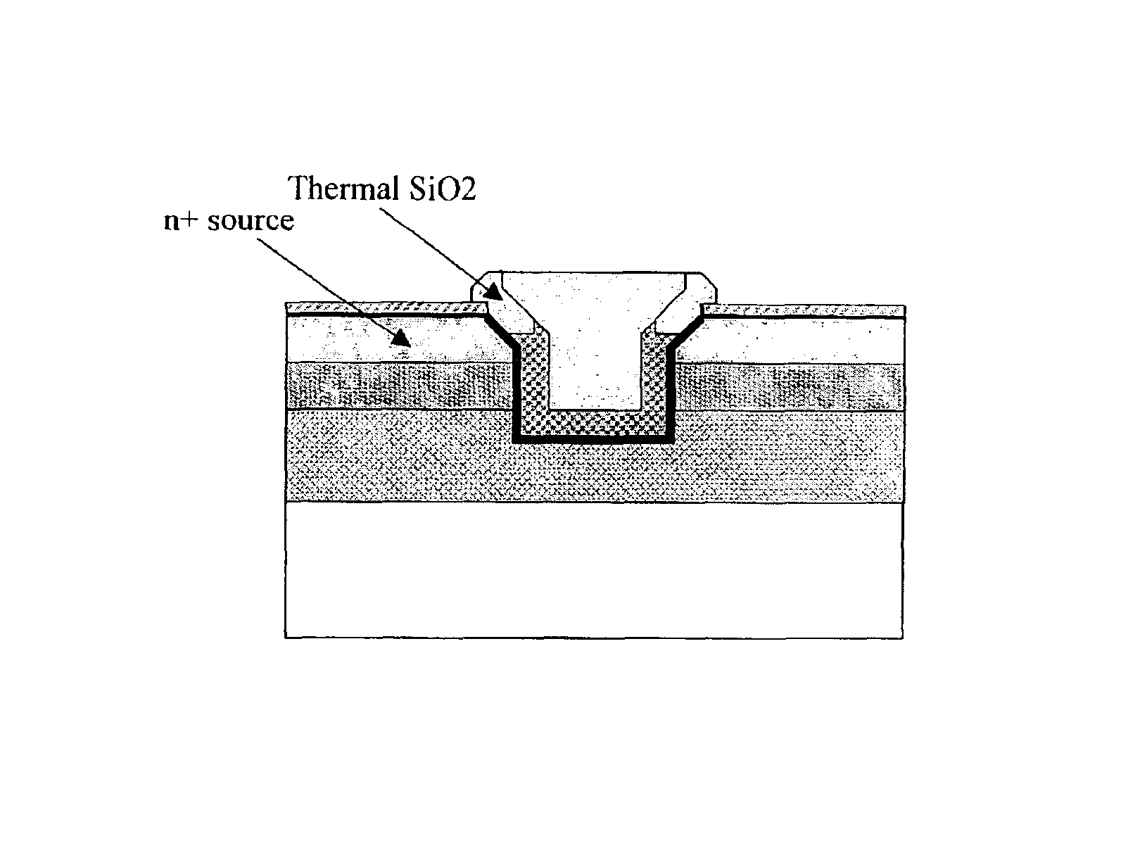
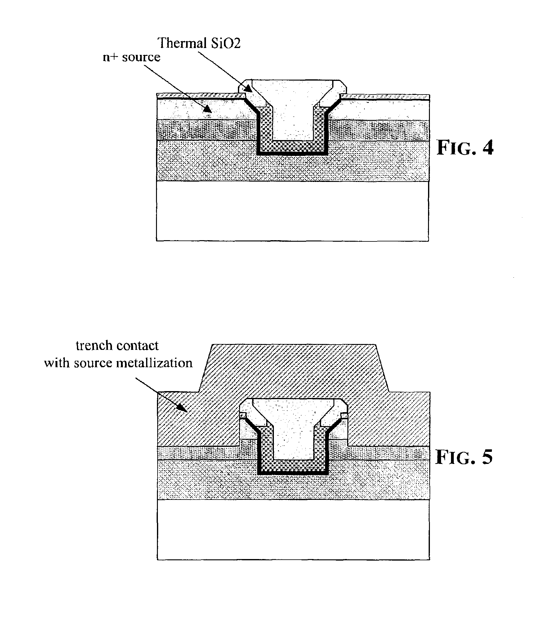
[0024]A pad oxide or a pad oxide-nitride is grown and a layer of pyrolytic nitride (SiN / ox) is deposited over the surface of the second epitaxial layer, for example, a p-epitaxy. This is preferably carried out by a heat treatment in an oven in presence of oxygen for obtaining an oxide layer (≈10 to 20 nm), and eventually in the presence of nitrogen for obtaining an oxy-nitride layer. This is followed by deposition of a pyrolytic layer Si3N4 (30 to 70 nm) in an oven.

[0025]Gate trench photolithography is performed for forming a definition mask for the trench windows (strips) within the active area. The stack SiN / ...

second embodiment (

Diffused Body):

[0048]An epitaxial layer of a first type of conductivity is formed on a semiconductor silicon mono-crystalline substrate, and the edge structure and the active area are formed according to any technique of the prior art. Photolithography of the gate trenches includes forming a definition mask for the trench strips within the active area, and the silicon is plasma etched.

[0049]The next step includes countersinking the upper part of the trenches. This represents an essential requirement of the process of the invention and any technique suitable to produce the desired countersinking may be used. For example, plasma etching the silicon crystal may be done while controlling the tilt angle to obtain a countersinking of about 50÷100 nm at the rim of the cross section profile of the trench. An appropriate tilt for inclining (beveling) the upper portion of the walls of the trench may be carried out during or at the end of the etching process.

[0050]Growth of the gate dielectric...


PUM


Abstract

A process for forming a trench gate power MOS transistor includes forming an epitaxial layer having a first type of conductivity on a semiconductor substrate, and forming a body region having a second type of conductivity on the epitaxial layer. A gate trench is formed in the body region and in the epitaxial layer. The process further includes countersinking upper portions of the gate trench, and forming a gate dielectric layer on surfaces of the gate trench including the upper portions thereof. A gate conducting layer is formed on surfaces of the gate dielectric layer for defining a gate electrode. The gate conducting layer has a thickness that is insufficient for completely filling the gate trench so that a residual cavity remains therein. The residual cavity is filled with a filler layer. The gate conducting layer is removed from an upper surface of the body region while using the filler layer as a self-aligned mask. The edge surfaces of the gate conducting layer are oxidized. Source regions are formed by implanting dopants in the body region while using the oxidized edge surfaces as a self-aligned mask, and the implanted dopants are diffused in the body region.

Description

FIELD OF THE INVENTION[0001]The present invention relates to fabrication techniques for integrated devices, and in particular, to a fabrication technique for a trench gate power MOS transistor.BACKGROUND OF THE INVENTION[0002]Designing and fabricating power VDMOS transistors having scaled dimensions but with high current capabilities is limited with respect to nested geometries being formed within an elementary unit in an active area. Moreover, even if it were possible to accurately align structures in submicron spaces, certain contributions to the ON-resistance of the integrated device would still limit the level of performance that can be achieved.[0003]A typical example is the JFET contribution to the resistance in the active area, which depends on the separation distance between contiguous body diffusions. Making two contiguous elementary structures closer together leads to an increase in the packing density, and thus the active perimeter of the device per unit area. At the same...

Claims


Application Information

Patent Timeline
Patent Type & Authority Patents(United States)
IPC IPC(8): H01L21/02H01L29/66H01L21/336H01L29/78H01L29/49H01L29/40
CPCH01L29/7813H01L29/4933
Inventor CURRO', GIUSEPPEFAZIO, BARBARA
Owner STMICROELECTRONICS SRL
Why Eureka
Try Eureka