Supercharge Your Innovation With Domain-Expert AI Agents!

Memory device and data reading method

a memory device and data reading technology, applied in the field of memory devices, can solve the problems that damaged auxiliary data also needs an additional redundancy circuit for repair

Active Publication Date: 2012-03-06
POWERCHIP SEMICON MFG CORP
View PDF5 Cites 0 Cited by
  • Summary
  • Abstract
  • Description
  • Claims
  • Application Information

AI Technical Summary

Benefits of technology

Enables efficient data reading and reduces the necessity for additional redundancy circuits, simplifying the NAND flash memory operation and eliminating the need for wafer sorting of auxiliary data cells, thereby improving operational efficiency and reducing complexity.

Problems solved by technology

Compared with the main data, damaged auxiliary data also needs an additional redundancy circuit for repair even though the memory cells used by the auxiliary data occupies a minimal part of the total memory array.

Method used


Image

  • Memory device and data reading method
  • Memory device and data reading method
  • Memory device and data reading method

Examples


Embodiment Construction

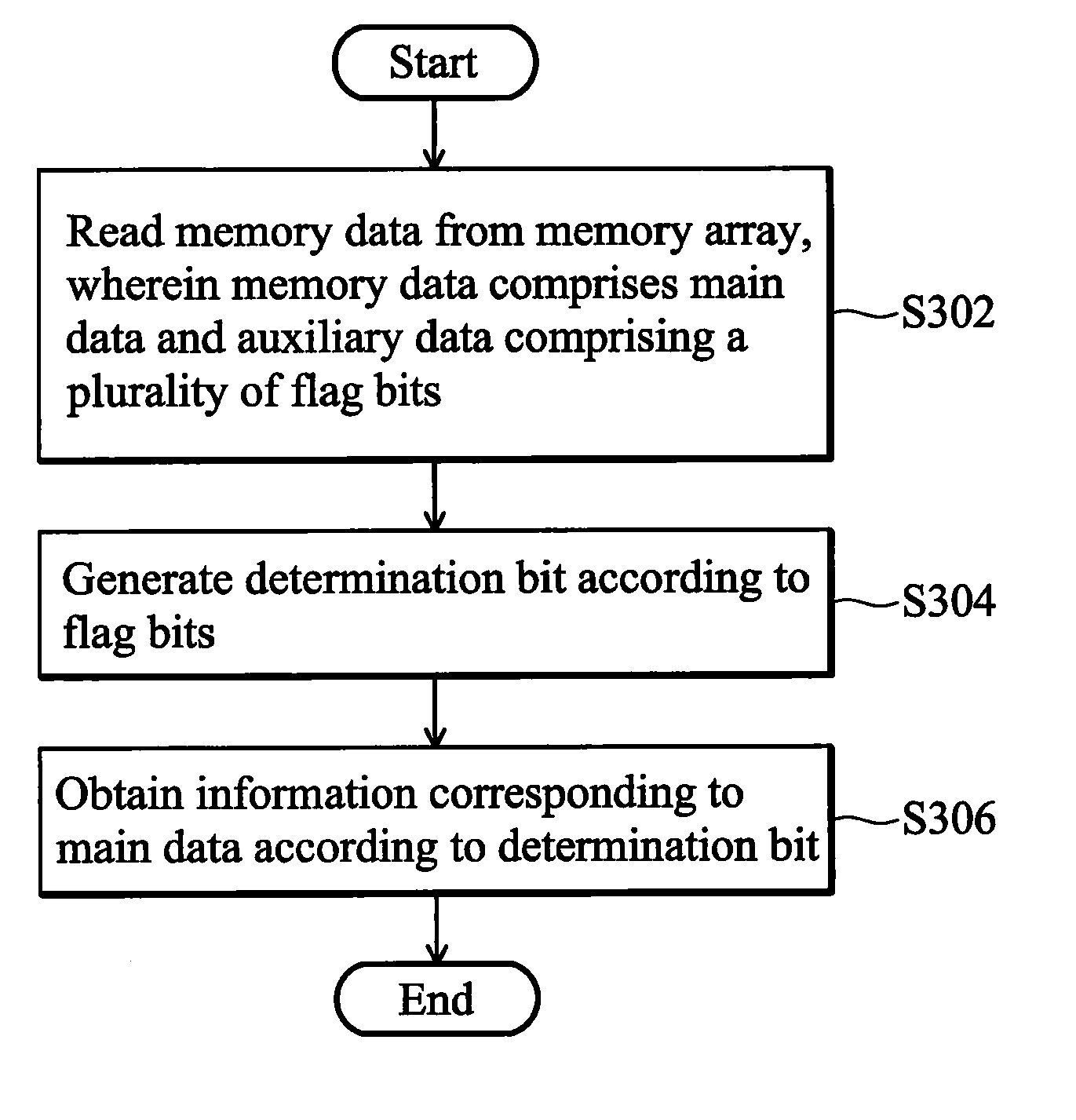
[0016]The following description is of the best-contemplated mode of carrying out the invention. This description is made for the purpose of illustrating the general principles of the invention and should not be taken in a limiting sense. The scope of the invention is best determined by reference to the appended claims.

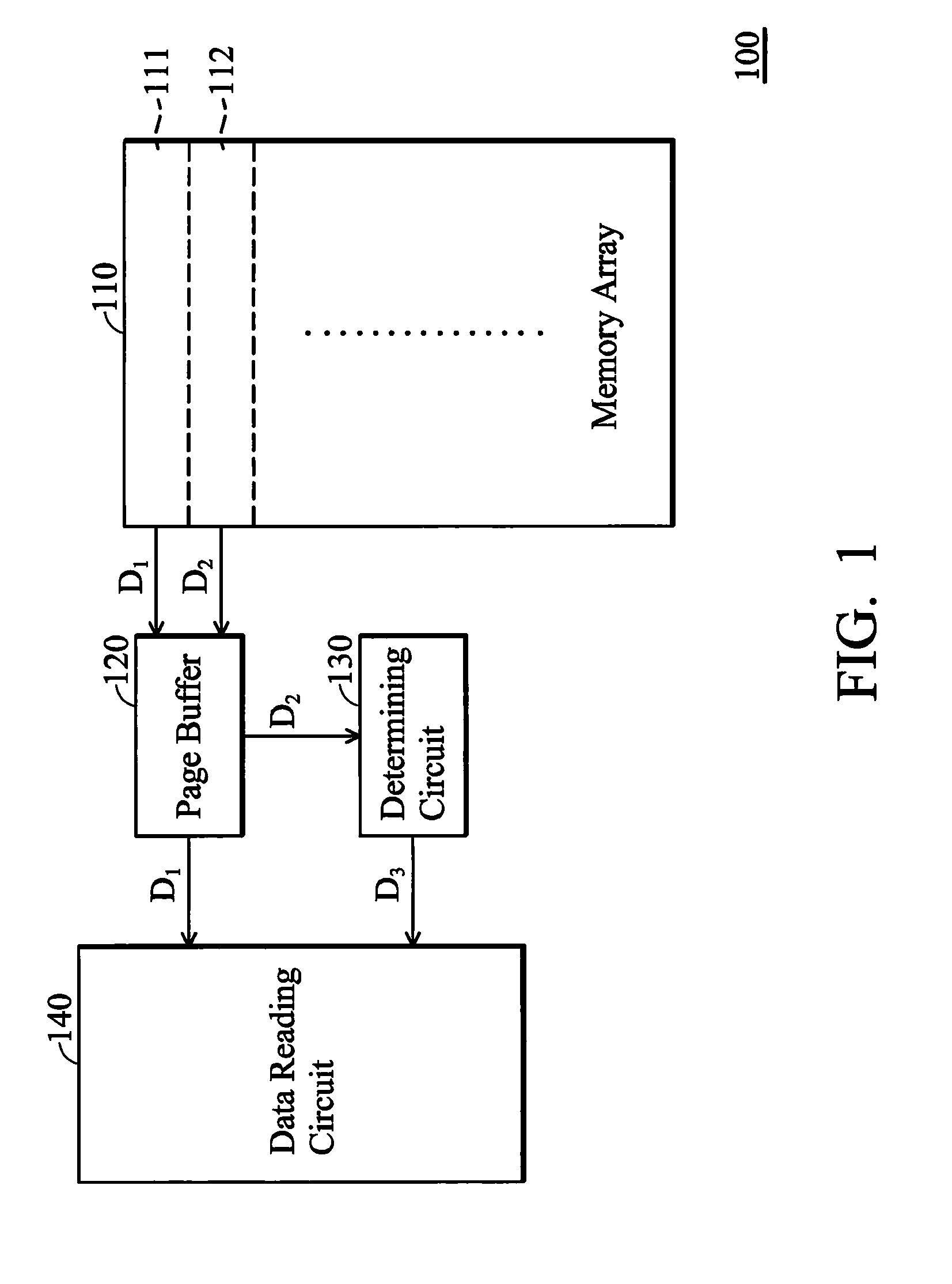
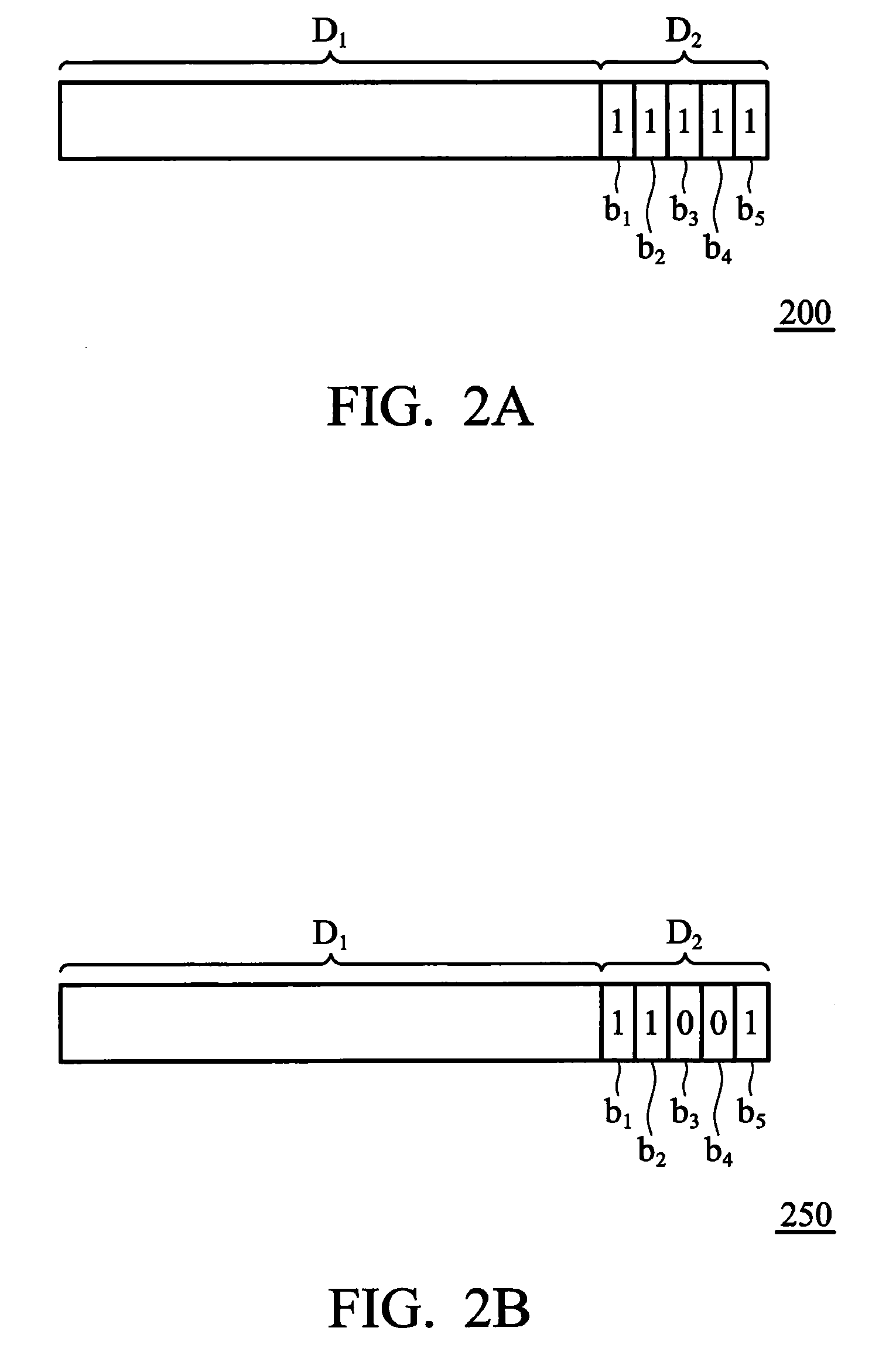
[0017]FIG. 1 shows a memory device 100 according to an embodiment of the invention. The memory device 100 comprises a memory array 110, a page buffer 120, a determining circuit 130 and a data reading circuit 140. As shown in FIG. 1, the memory array 110 is an NAND flash which is formed by a plurality of multi level cells, and the memory array 110 may be divided into a plurality of page units, such as a page 111, a page 112 and so on. In the memory array 110, each page unit may comprise a main data and an auxiliary data corresponding to the main data, wherein the auxiliary data is a multi-bit data. A main data D1 and an auxiliary data D2 may be transmitted to the page b...


PUM


Abstract

A memory device is provided. The memory device includes a memory array formed by a plurality of multi level cells, a determining circuit and a data reading circuit. The memory array includes a plurality of page units, each including a main data and an auxiliary data corresponding to the main data, wherein the auxiliary data includes a plurality of flag bits. The determining circuit generates a determination bit according to the flag bits. The data reading circuit obtains information corresponding to the main data according to the determination bit.

Description

CROSS REFERENCE TO RELATED APPLICATIONS[0001]This Application claims priority of Taiwan Patent Application No. 97100537, filed on Jan. 7, 2008, the entirety of which is incorporated by reference herein.BACKGROUND OF THE INVENTION[0002]1. Field of the Invention[0003]The invention relates to a memory device, and more particularly to an NAND flash with odd flag bits.[0004]2. Description of the Related Art[0005]In general, the data stored in an NAND flash may comprise main data and annotated data, wherein each annotated data is an auxiliary data of the main data. For example, the auxiliary data may be an error correction code or a memory cell failed symbol, wherein the auxiliary data is designed by its manufacturer according different practical applications.[0006]After a wafer sorting process is performed, an NAND flash needs an additional redundancy circuit to replace a failed cell therein, so that the NAND flash may be operated normally. For example, Park (U.S. Pat. No. 5,694,359) dis...

Claims


Application Information

Patent Timeline
Patent Type & Authority Patents(United States)
IPC IPC(8): G06F12/00
CPCG06F12/0246G11C16/0483G11C16/10
Inventor TU, CHUN-YITSENG, TE-CHANGARAKAWA, HIDEKINAKAYAMA, TAKESHI
Owner POWERCHIP SEMICON MFG CORP
Features
  • R&D
  • Intellectual Property
  • Life Sciences
  • Materials
  • Tech Scout
  • Unparalleled Data Quality
  • Higher Quality Content
  • 60% Fewer Hallucinations
Learn More