Endurance and retention flash controller with programmable binary-levels-per-cell bits identifying pages or blocks as having triple, multi, or single-level flash-memory cells

a flash controller and memory technology, applied in the field of flash controllers, can solve the problems of low endurance, low endurance, and failure rate of high-density cells, and achieve the effect of reducing the number of program-erase cycles before the cell wears out and fails

Inactive Publication Date: 2015-09-01
SUPER TALENT TECH CORP
View PDF14 Cites 109 Cited by
  • Summary
  • Abstract
  • Description
  • Claims
  • Application Information

AI Technical Summary

Problems solved by technology

However, since flash memory chips are block-addressable rather than randomly-accessible, flash is not as easy to use for a cache as DRAM or SRAM.
Thus higher-density cells tend to have a lower reliability.
Programming must be more exact since the voltage range of any one logic state is smaller, and this precise programming may require more time, and may create more wear on the memory cells, resulting in a lower endurance, or number of program-erase cycles before the cell wears out and fails.
As process technologies shrink the size of the flash memory cell, insulating oxide layers are also shrunk, causing the memory cells to wear out and fail after a smaller number of program-erase cycles.
Newer flash chips may only allow for a few thousand or even a few hundred program-erase cycles before the cells become unreliable.
Cell leakage also may become a problem.

Method used


Image

  • Endurance and retention flash controller with programmable binary-levels-per-cell bits identifying pages or blocks as having triple, multi, or single-level flash-memory cells
  • Endurance and retention flash controller with programmable binary-levels-per-cell bits identifying pages or blocks as having triple, multi, or single-level flash-memory cells
  • Endurance and retention flash controller with programmable binary-levels-per-cell bits identifying pages or blocks as having triple, multi, or single-level flash-memory cells

Examples


Embodiment Construction

[0043]The present invention relates to an improvement in adaptive Multi-Level-Cell (MLC) flash chips. The following description is presented to enable one of ordinary skill in the art to make and use the invention as provided in the context of a particular application and its requirements. Various modifications to the preferred embodiment will be apparent to those with skill in the art, and the general principles defined herein may be applied to other embodiments. Therefore, the present invention is not intended to be limited to the particular embodiments shown and described, but is to be accorded the widest scope consistent with the principles and novel features herein disclosed.

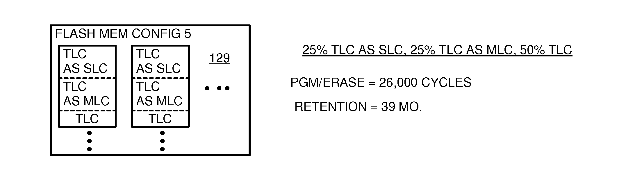
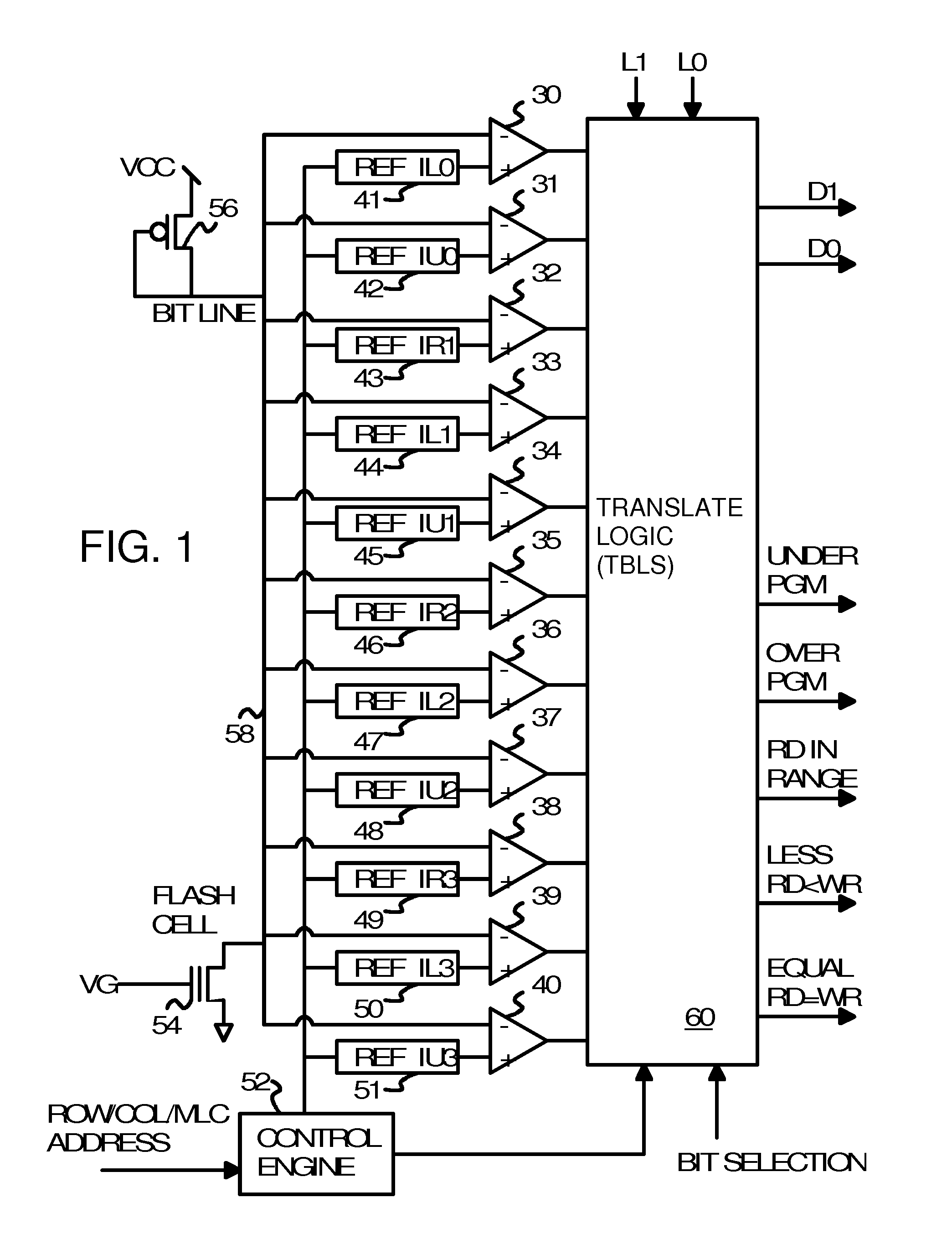
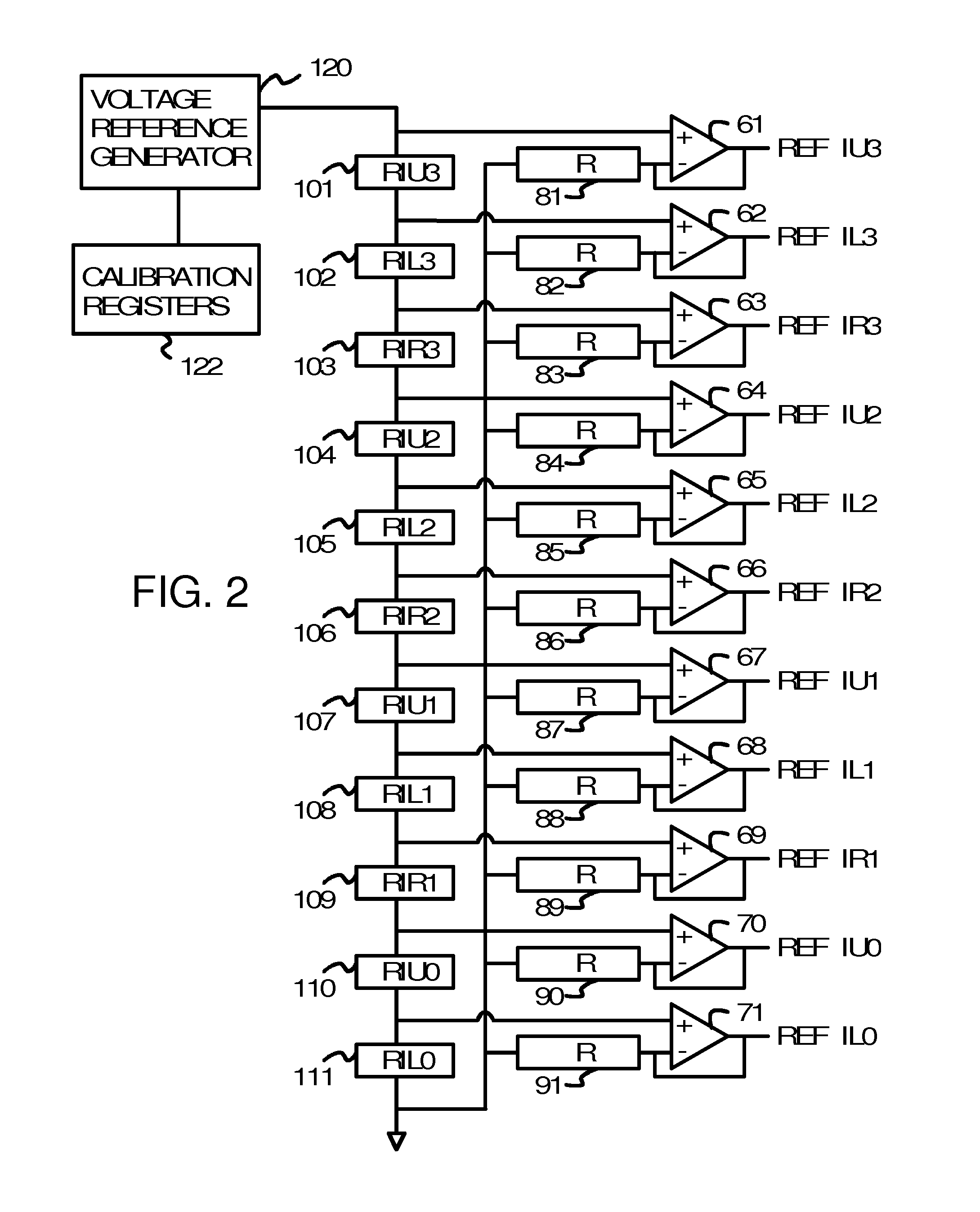
[0044]FIG. 1 shows multi-level voltage sensing of a MLC cell. The example of FIGS. 1-2 show a 2-bit, 4-state MLC, but other examples could be devised for other sizes, such as 4-bit, 16-state QLC memory.

[0045]A flash-memory chip has an array of flash cells arranged in rows and columns that are selectable by ...


PUM


Abstract

An retention flash controller reads assigned-level bits from a bad block / erase count table or from a page status table that indicate when flash memory cells operate as Triple-Level-Cell (TLC), Multi-Level-Cell (MLC), or Single-Level-Cell (SLC). Pages that fail as TLC or MLC are downgraded for use as SLC pages by changing the assigned-level bits. The level bits adjust truth tables used by translation logic that receives inputs from voltage comparators reading a bit line. The range of voltages for each logic level may be adjusted by the truth tables or by programmable registers. The programming voltage or programming pulses may be adjusted to increase endurance and the number of permitted program-erase cycles while reducing retention times before a refresh is needed of the flash cells. Mixed configurations of flash memory have MLC blocks and MLC as SLC blocks, or other combinations.

Description

RELATED APPLICATION[0001]This application is a continuation-in-part (CIP) of “Super-Endurance Solid-State Drive with Endurance Translation Layer (ETL) and Diversion of Temp Files for Reduced Flash Wear”, U.S. Ser. No. 13 / 540,569, filed on Jul. 2, 2012.[0002]This application is a continuation-in-part (CIP) of “Virtual Memory Device (VMD) Application / Driver with Dual-Level Interception for Data-Type Splitting, Meta-Page Grouping, and Diversion of Temp Files to Ramdisks for Enhanced Flash Endurance”, U.S. Ser. No. 13 / 730,797, filed on Dec. 28, 2012.FIELD OF THE INVENTION[0003]This invention relates to Solid-State Drive (SSD) systems, and more particularly to flash controllers that adaptively program single or multi-level cells.BACKGROUND OF THE INVENTION[0004]Mass storage is used to store large amounts of data that is typically copied to a faster random-access memory such as a dynamic-random-access memory (DRAM) for use by a processor. While the processor's DRAM is randomly accessible,...

Claims


Application Information

Patent Timeline
Patent Type & Authority Patents(United States)
IPC IPC(8): G06F12/00G06F13/00G06F12/02G06F13/28G11C16/10G11C13/00G11C29/00
CPCG11C16/10G06F12/0246G06F2212/7203G06F2212/7208G11C13/0004G11C29/765G11C2211/5641
Inventor YU, FRANKMA, ABRAHAM C.CHEN, SHIMONCHANG, YAO-TSE
Owner SUPER TALENT TECH CORP
Why Eureka
Try Eureka