Touch sensing display panel, touch sensing color filter and fabricating method thereof
a touch sensing display panel and touch sensing technology, applied in the field of display panel, color filter, and fabricating methods thereof, can solve the problems single-side design still has the problem of complicated fabrication process and limited resolution, and achieves the effect of better touch sensing resolution and touch sensing sensitivity
- Summary
- Abstract
- Description
- Claims
- Application Information
AI Technical Summary
Benefits of technology
Problems solved by technology
Method used
Image
Examples
first embodiment
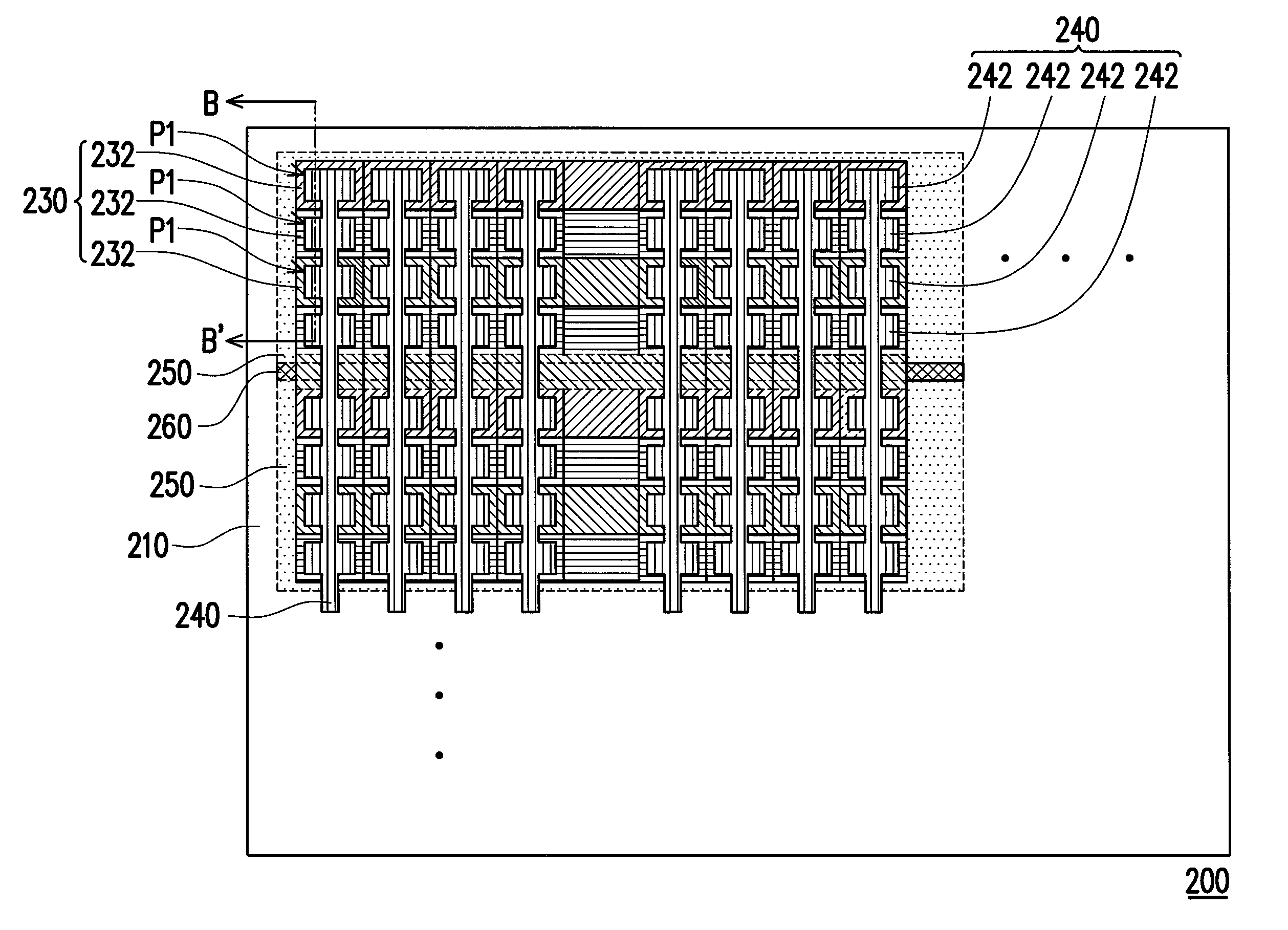
[0051]FIG. 2A illustrates a top view of a touch sensing color filter according to the first embodiment of the present invention, and FIG. 2B illustrates a cross-sectional view of the touch sensing color filter along the line BB′ in FIG. 2A. For clarity, FIG. 2A mainly illustrates a structure of a sensing electrode, and the layers thereon, such as a third dielectric layer and a common electrode layer, are not shown. FIG. 2B illustrates the arrangement of a substrate and each layer in detail.
[0052]In this embodiment, a touch sensing color filter 200 comprises a substrate 210, a black matrix 220, a color filter layer 230, and a second sensing electrode layer 240, wherein a connection between each element of the touch sensing color filter 200 is shown in FIGS. 2A and 2B.
[0053]The connection between each element of the touch sensing color filter 200 is described in detail as follows.
[0054]In this embodiment, a material of the substrate 210 comprises an inorganic transparent material (e.g...
second embodiment
[0073]FIG. 3A illustrates a top view of a touch sensing color filter according to the second embodiment of the present invention, and FIG. 3B illustrates a cross-sectional view of the touch sensing color filter along the line CC′ in FIG. 3A. For clarity, FIG. 3A mainly illustrates a structure of a sensing electrode, and the layers thereon, such as a first dielectric layer, a third dielectric layer, and a common electrode layer, are omitted. FIG. 3B illustrates the arrangement of a substrate and each layer in detail.
[0074]Referring to FIGS. 2A, 2B, 3A, and 3B, a structure of a touch sensing color filter 300 is similar to that of the touch sensing color filter 200, and the redundant descriptions are not repeated hereafter. The difference lies in that the touch sensing color filter 300 further comprises a first dielectric layer 310, wherein the first dielectric layer 310 covers the color filter layer 230 and the black matrix 220, and the second sensing electrode layer 240 is disposed o...
third embodiment
[0078]FIG. 4A illustrates a top view of a touch sensing color filter according to the third embodiment of the present invention, and FIG. 4B illustrates a cross-sectional view of the touch sensing color filter along the line DD′ in FIG. 4A. For clarity, FIG. 4A mainly illustrates a structure of a sensing electrode, and the layers thereon, such as a second dielectric layer, a third dielectric layer, and a common electrode layer, are omitted. FIG. 4B illustrates the arrangement of a substrate and each layer in detail.
[0079]Referring to FIGS. 4A and 4B, a touch sensing color filter 400 in this embodiment is formed by varying a sequence of the layers of the touch sensing color filter 200. Accordingly, the same elements are indicated by the same reference numbers. Moreover, the touch sensing color filter 400 further comprises a second dielectric layer 410. The second dielectric layer 410 is disposed between the black matrix 220 and the substrate 210, and the second sensing electrode laye...
PUM
 Abstract
Description
Claims
Application Information


