Organic-inorganic lighting device and a method for fabricating the same
a technology of organic-inorganic lighting and lighting devices, which is applied in the field of organic-inorganic lighting devices, can solve the problems of affecting the efficiency of the device, the number of electrons and holes in the device to be unbalanced, and the disadvantage of the transmission of holes, so as to achieve the effect of low electron mobility and greatly reduced fabrication costs
- Summary
- Abstract
- Description
- Claims
- Application Information
AI Technical Summary
Benefits of technology
Problems solved by technology
Method used
Image
Examples
first embodiment
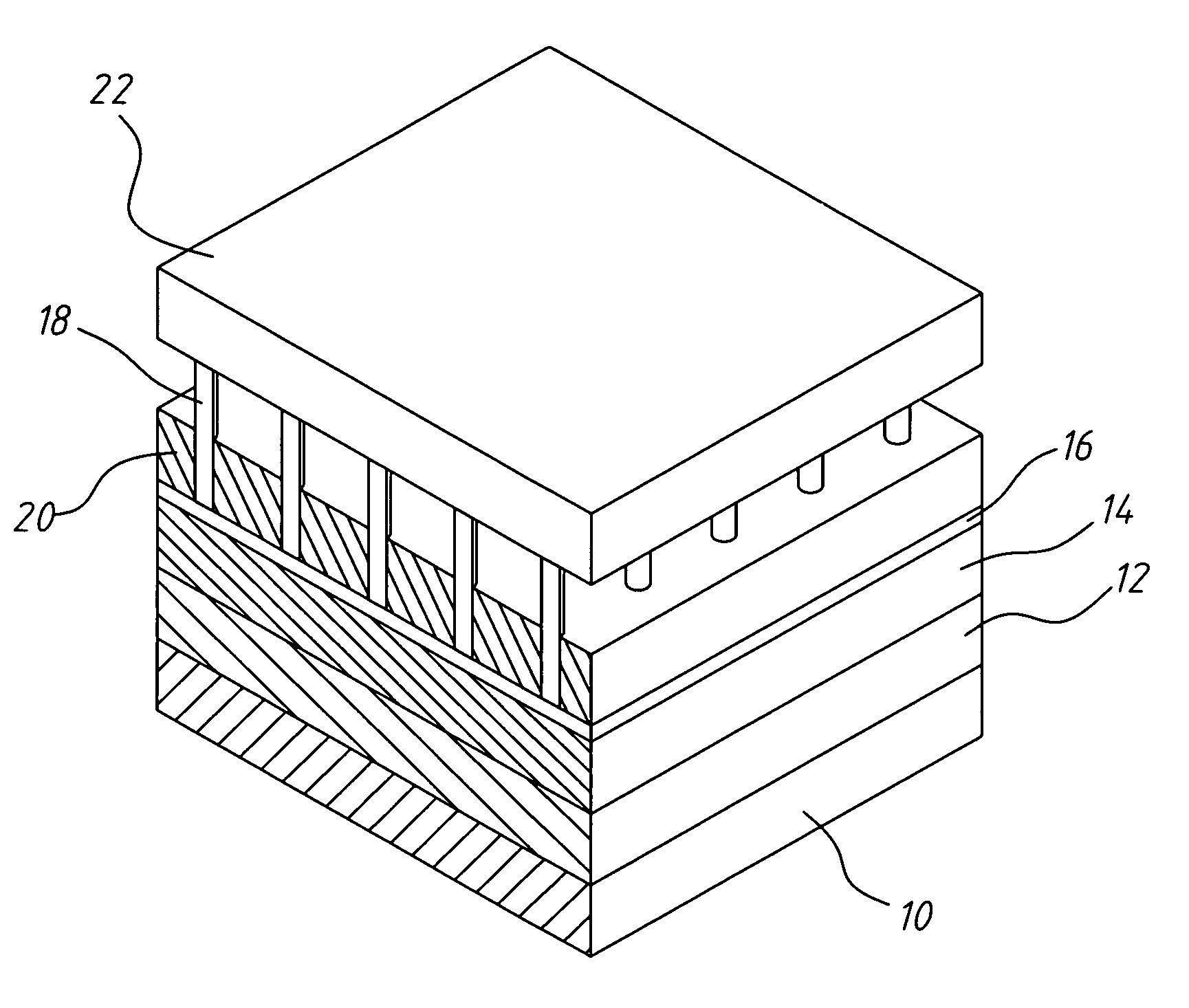
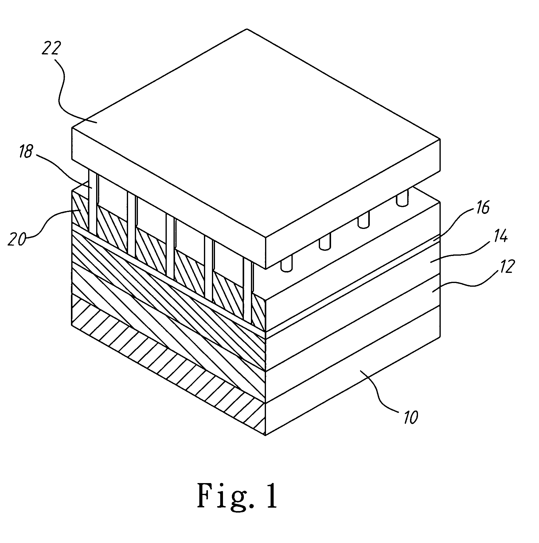
[0033]Refer to FIGS. 3(a)-3(k) for the method to fabricate the organic-inorganic lighting device of the As shown in FIG. 3(a), an insulation substrate 10 is provided firstly. Next, a first electrode layer 12, an organic conductive thin-film layer 14 and a seed layer 16 are sequentially formed on the insulation substrate 10. The organic conductive thin-film layer 14 is fabricated using one of the following methods: spin-coating method, dip-coating method, or ink printing method. The spin-coating method, dip-coating method and ink printing method require one of the following solutions: chloroform, dichloromethane, toluene, tetrahydrofuran, 1,2-dichlorobenzene, 1,4-dichlorobenzene, chlorobenzene, or n-hexane.
[0034]The seed layer 16 is fabricated using one of the following methods: spin-coating method, dip-coating method, evaporation method, sputtering method, atomic layer deposition method, electrochemical deposition method, pulsed laser deposition method, or metalorganic chemical vap...
second embodiment
[0040]Refer to FIG. 4 for the present invention. The second embodiment is different from the first embodiment in that the first electrode layer 12 is divided into a plurality of first electrode blocks 24, and the first electrode blocks 24 are arranged equidistantly. The organic conductive thin-film layer 14 and the seed layer 16 are respectively divided into a plurality of organic blocks 26 and seed blocks 28; the array of micro and nano zinc oxide wire 18 is divided into a plurality of groups of micro array of zinc oxide 30, and the second electrode layer 22 is divided into a plurality of second electrode blocks 32. An organic block 26, a seed block 28, and a group of micro array of zinc oxide 30, are formed on each first electrode block 24 in order. The insulation layer 20 covers the seed layer 16 and the insulation substrate 10, and the top surface of the insulation layer 20 is lower than the tips of the array of micro and nano zinc oxide wire 18.
[0041]Refer to FIGS. 5(a)-5(e) fo...
third embodiment
[0042]Refer to FIG. 6 for the present invention. The third embodiment is different from the second embodiment in that a conductive substrate 34 replaces the insulation substrate 10 and the first electrode layer 12. The conductive substrate 34 has a plurality of conductive blocks 36 arranged equidistantly. An organic block 26, a seed block 28, and a group of micro array of zinc oxide 30, are formed on the each conductive block 36 in order.
[0043]Refer to FIGS. 7(a)-7(e) for the method of fabricating the organic-inorganic lighting device of the third embodiment. Firstly, as shown in FIG. 7(a), a conductive substrate 34 having a plurality of conductive blocks 36 arranged equidistantly is provided. Next, an organic block 26 and a seed layer 28 are sequentially formed on each conductive block 36. The steps shown in FIG. 7(b) to FIG. 7(e) are identical to the steps shown in FIG. 5(b) to FIG. 5(e), and have been described previously so will not be reiterated.
[0044]Below is a description of ...
PUM
| Property | Measurement | Unit |
|---|---|---|
| thickness | aaaaa | aaaaa |
| thickness | aaaaa | aaaaa |
| thickness | aaaaa | aaaaa |
Abstract
Description
Claims
Application Information


