Display device having light-emitting element and liquid crystal element and method for driving the same

a technology of liquid crystal elements and display devices, which is applied in static indicating devices, non-linear optics, instruments, etc., can solve problems such as reducing contrast, and achieve the effects of reducing power consumption, reducing light leakage, and improving contras

Active Publication Date: 2012-04-17
SEMICON ENERGY LAB CO LTD
View PDF42 Cites 29 Cited by
  • Summary
  • Abstract
  • Description
  • Claims
  • Application Information

AI Technical Summary

Benefits of technology

[0007]It is an object of the present invention to provide a display device in which a problem of light leakage from a liquid crystal element in black display is overcome and the contrast is improved.
[0022]In a conventional liquid crystal display device, a plurality of pixels use the same backlight as a light-emitting source. Therefore, a malfunction is generated, in which, when a backlight is turned off for a pixel displaying black, all other pixels also display black. However, in the present invention, a backlight is provided in each pixel; therefore, a light-emitting element that is a backlight can be turned off when a black gray scale is displayed, and reduction in contrast due to light leakage from a liquid crystal element can be prevented.

Problems solved by technology

Therefore, even when black is intended to be displayed, light leaks from a liquid crystal element, and completely black display cannot be performed, which leads to the reduced contrast.

Method used


Image

  • Display device having light-emitting element and liquid crystal element and method for driving the same
  • Display device having light-emitting element and liquid crystal element and method for driving the same
  • Display device having light-emitting element and liquid crystal element and method for driving the same

Examples


embodiment mode 1

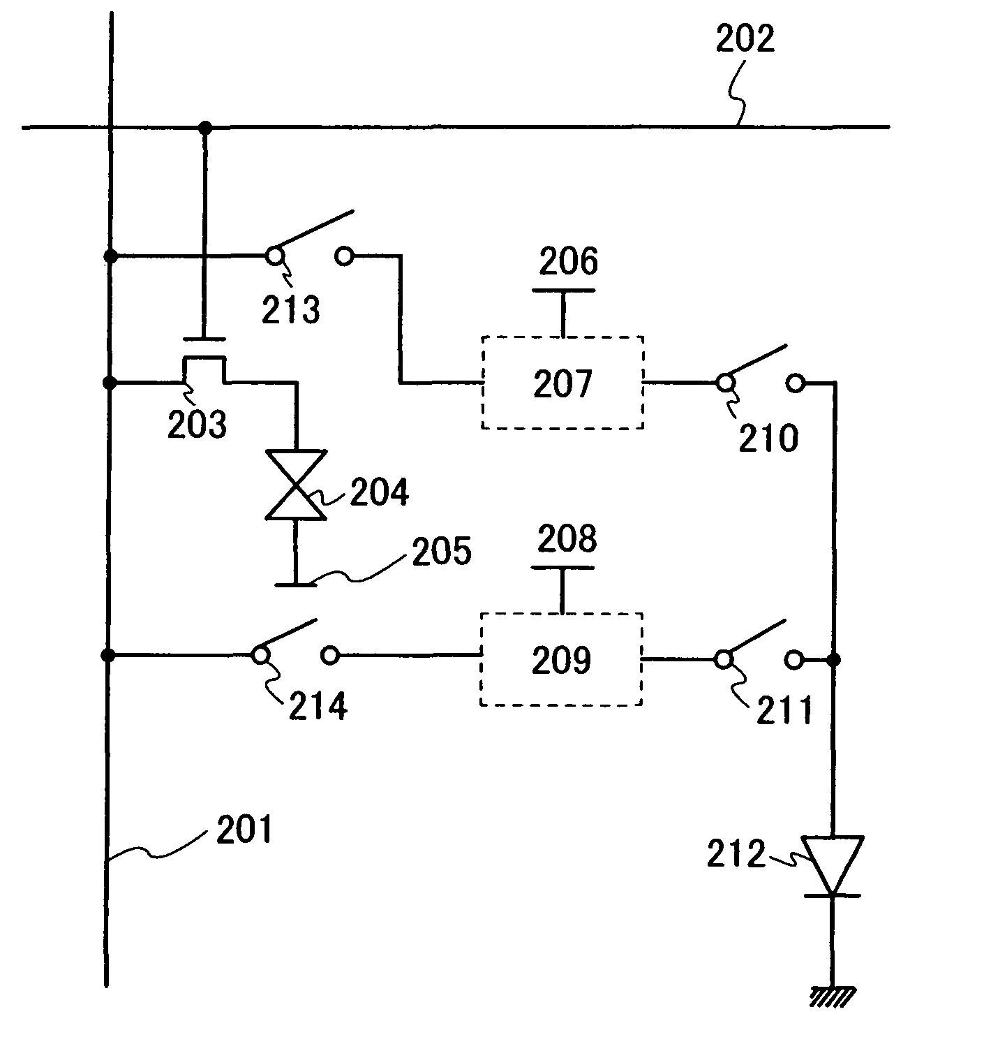
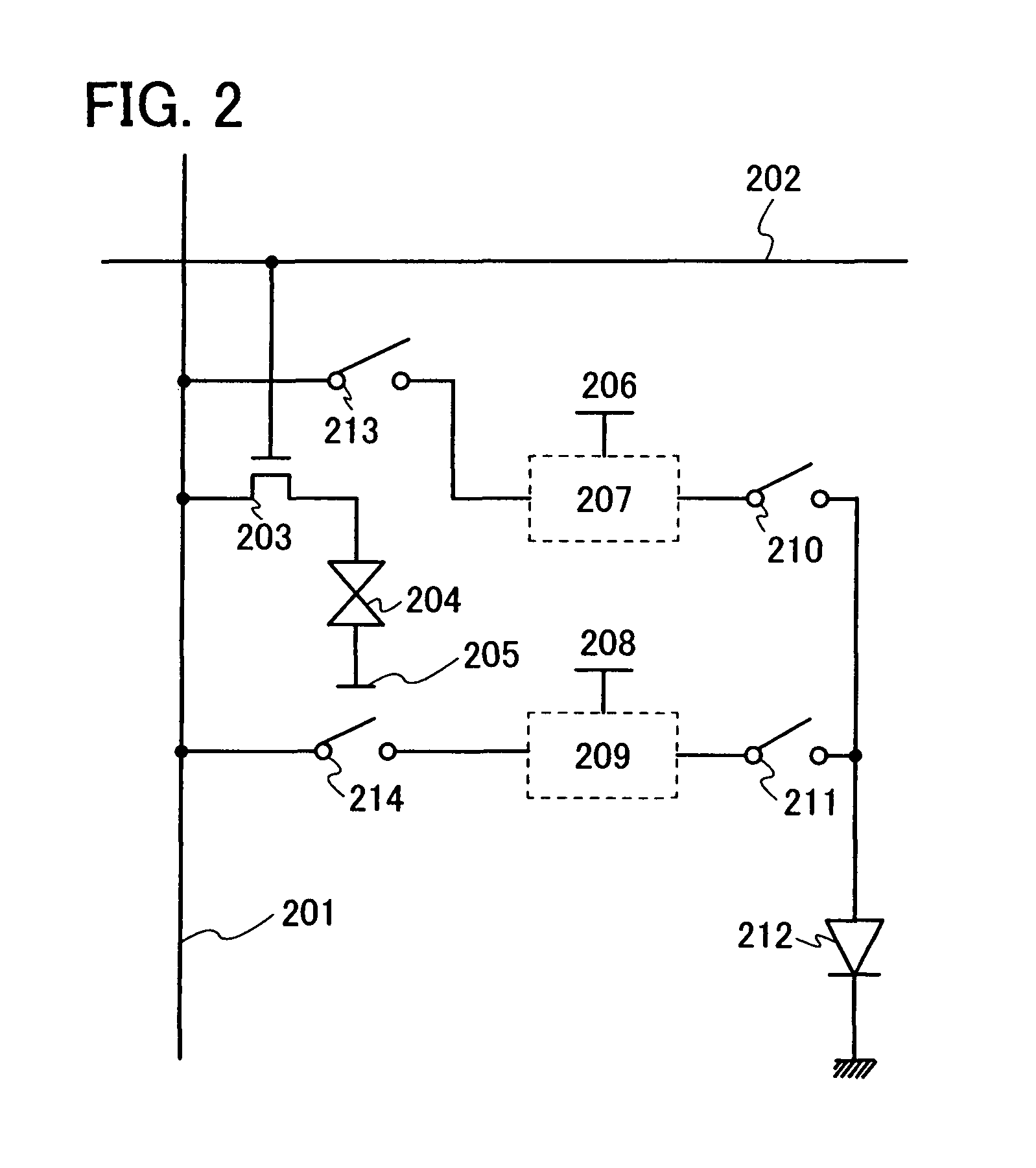
[0040]FIG. 2 schematically shows one embodiment mode of a pixel included in a display device of the present invention. In a circuit shown in FIG. 2, a data line 201 and a scanning line 202 are provided; a transistor 203 which performs writing to a liquid crystal element 204 and a counter electrode 205 are provided; a light-emitting element 212 used as a backlight, and a first comparator 207 and a second comparator 209 are provided; and a first switch 213 for writing a data signal into the first comparator 207 and a second switch 214 for writing a data signal into the second comparator 209 are provided. A first reference potential 206 that is compared with a data potential is input to the first comparator 207, and a second reference potential 208 that is compared with a data potential is input to the second comparator 209. In addition, a third switch 210 and a fourth switch 211, by which it is determined which of the first comparator 207 and the second comparator 209 is selected to t...

embodiment mode 2

[0067]This embodiment mode will explain a configuration of a pixel circuit which is different from that of the above embodiment mode. FIG. 6 schematically shows a circuit in which one comparator is removed from the circuit of Embodiment Mode 1. In the circuit shown in FIG. 6, a data line 601 and a scanning line 602 are provided. In addition, a transistor 603 which performs writing to a liquid crystal element 604 and a counter electrode 605 are provided. Further, a light-emitting element 612 used as a backlight is provided. A first switch 613 which writes a data signal into a comparator 608 is provided. A first reference potential 606 and a second reference potential 607 which are compared with a data potential are provided. In addition, a second switch 609 and a third switch 610, by which it is determined which of positive and negative outputs is output from the comparator to the light-emitting element, are provided.

[0068]The components in the circuit shown in FIG. 6 are connected a...

embodiment mode 3

[0080]FIG. 11A shows one mode of a display device of this embodiment mode. Over a glass substrate 1101, a base film 1115 is formed, and a liquid crystal element driving transistor 1113 and a light-emitting element driving transistor 1114 are formed thereover. The liquid crystal element driving transistor 1113 includes a first impurity region 1117a and a second impurity region 1117b. A first channel region 1116a is formed between the first impurity region 1117a and the second impurity region 1117b. A gate insulating film 1118 is formed over the first impurity region 1117a, the second impurity region 1117b, and the first channel region 1116a. A first gate electrode 1119a is formed over the gate insulating film 1118. Similarly, the light-emitting element driving transistor 1114 includes a third impurity region 1117c and a fourth impurity region 1117d. A second channel region 1116b is formed between the third impurity region 1117c and the fourth impurity region 1117d. The gate insulatin...


PUM


Abstract

It is an object to provide a display device in which a problem of light leakage from a liquid crystal element in black display is reduced or overcome and the contrast is improved. It is another object to provide a pixel circuit having a function to control a lighting state of a backlight based on each pixel. These objects are achieved by turning off a light-emitting element in display of a black gray scale, and by providing a light-emitting element in each pixel and providing, in a pixel circuit, a function to individually control lighting and non-lighting of the light-emitting element depending on a gray scale to perform display. When a backlight is provided in each pixel, a light-emitting element that is a backlight is turned off when a black gray scale is displayed, whereby reduction in contrast due to light leakage from a liquid crystal element can be prevented.

Description

BACKGROUND OF THE INVENTION[0001]1. Field of the Invention[0002]The present invention relates to a liquid crystal display device, and particularly, a structure of a pixel including a liquid crystal and a backlight.[0003]2. Description of the Related Art[0004]A liquid crystal display device is formed by a combination of a liquid crystal panel in which a liquid crystal is sandwiched between a pair of substrates and a lighting system called a backlight on a rear side of the liquid crystal panel. As for the liquid crystal panel, a simple matrix mode and an active matrix mode using a thin film transistor (TFT) are known (refer to Patent Document 1: Japanese Published Patent Application No. H9-90404). In either mode, a voltage which is applied to electrodes sandwiching the liquid crystal is controlled, and the quantity of transmitted light of the backlight which illuminates the entire surface of the liquid crystal panel is adjusted, whereby an image is displayed. Therefore, for example, a...

Claims


Application Information

Patent Timeline
Patent Type & Authority Patents(United States)
IPC IPC(8): G09G3/36
CPCG02F1/133603G09G3/3208G09G3/3426G09G3/3648G02F1/1362G09G2330/021G09G2300/046G09G2320/0238G09G2320/062G09G2320/066G09G3/36
Inventor KIMURA, HAJIMEYOSHIDA, YASUNORISHISHIDO, HIDEAKIUMEZAKI, ATSUSHIYANAGISAWA, MAKOTOYAMAZAKI, SHUNPEI
Owner SEMICON ENERGY LAB CO LTD
Why Eureka
Try Eureka