Supercharge Your Innovation With Domain-Expert AI Agents!

Semiconductor package including multiple chips and separate groups of leads

a technology of semiconductor packages and leads, applied in the direction of semiconductor/solid-state device details, semiconductor devices, electrical equipment, etc., can solve the problems of affecting all the semiconductor chips of the group, unable to reduce the total number of semiconductor packages mounted on the substrate, and the semiconductor package is considered defective, so as to reduce the space necessary for mounting, increase packaging yield, and save manufacturing costs

Active Publication Date: 2012-06-05
SAMSUNG ELECTRONICS CO LTD
View PDF19 Cites 3 Cited by
  • Summary
  • Abstract
  • Description
  • Claims
  • Application Information

AI Technical Summary

Benefits of technology

This design enhances packaging yield, reduces the number of packages needed, and increases data transfer speed by allowing parallel data input / output operations, while maintaining functionality even with defective chips.

Problems solved by technology

In the case of a semiconductor package that has a stacked structure of semiconductor chips, the semiconductor package is considered defective even when only one semiconductor chip is defective from among all the semiconductor chips in the semiconductor package.
Because a single group of lead pins or other package terminals are used by all of the semiconductor chips in the semiconductor package, a defect in one chip or elsewhere in the package (e.g., contact of neighboring wire bonds) may affect all the semiconductor chips of that group.
In the case of a semiconductor package with leads of a single group, at least one semiconductor package is necessary for each channel of a controller, and thus, it is impossible to reduce the total number of semiconductor packages mounted on a substrate.
Also, in the case of a semiconductor package with leads of a single group, the number of input / output leads is limited; and the semiconductor packages may be connected serially to each connection channel provided by the controller, and thus it is difficult to improve the speed of inputting / outputting data.

Method used


Image

  • Semiconductor package including multiple chips and separate groups of leads
  • Semiconductor package including multiple chips and separate groups of leads
  • Semiconductor package including multiple chips and separate groups of leads

Examples


Embodiment Construction

[0045]Hereinafter, selected examples of semiconductor packages and electrical connections implemented therein will be described in detail with reference to the accompanying drawings. It will be appreciated by those skilled in the art that the following discussion is for demonstration purposes, and should not be interpreted as a limitation. Other variances within the scope of this disclosure are also applicable.

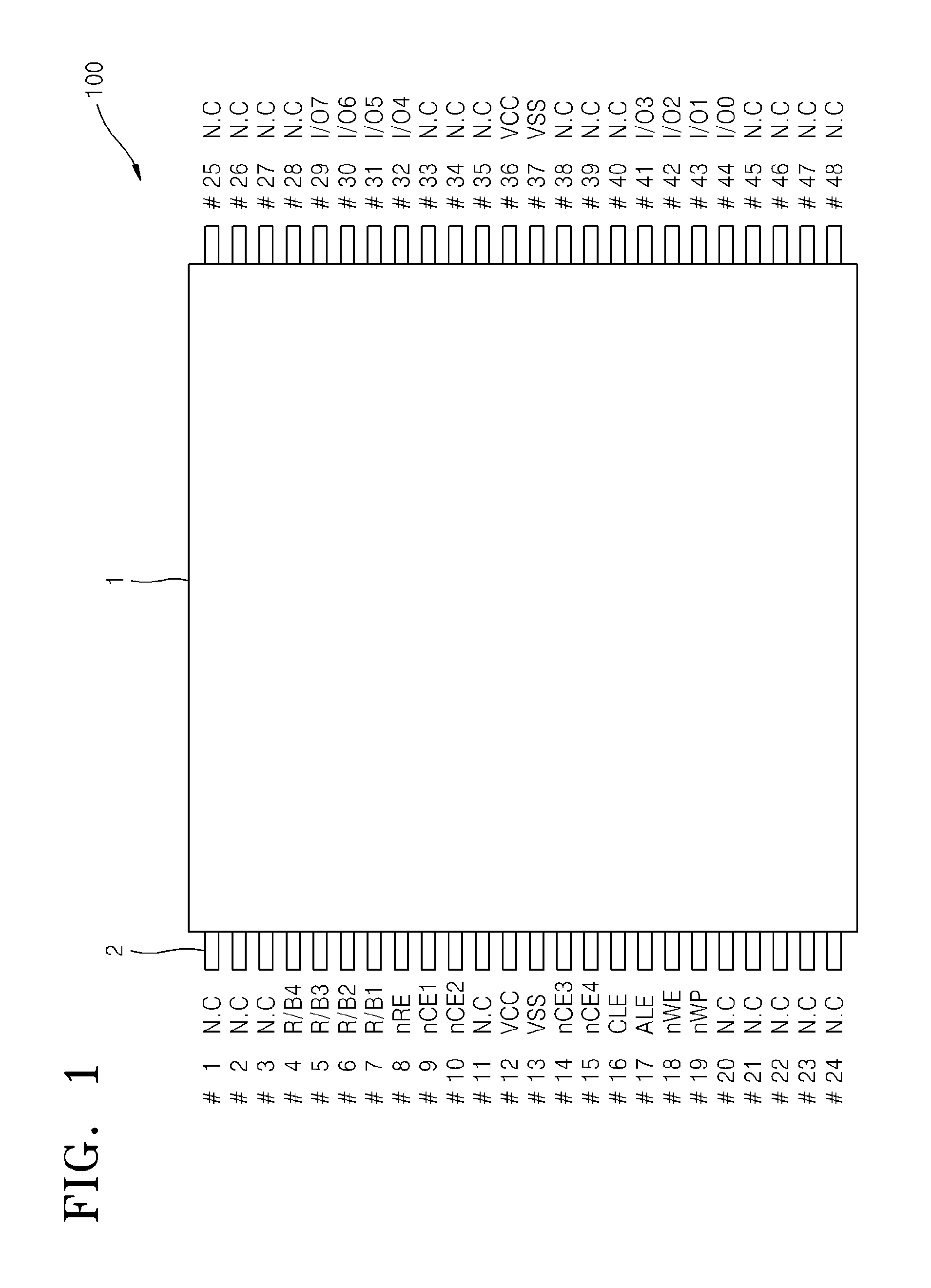
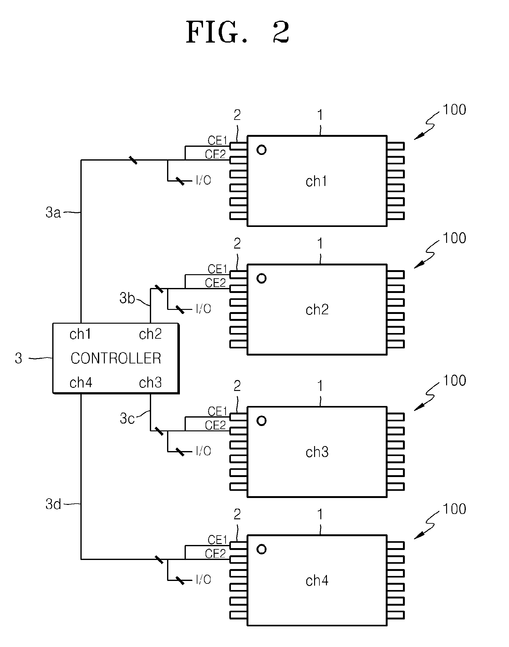
[0046]FIG. 1 is a plane view of the pin arrangement of a semiconductor package 100 having only one pin group, according to one example. FIG. 2 is a conceptual diagram illustrating a case where the semiconductor packages 100, such as shown in FIG. 1, are connected to a four-channel controller 3, according to another example. FIG. 3 is a conceptual diagram illustrating another example where the semiconductor packages 100, such as shown in FIG. 1, are connected to an eight-channel controller 3.

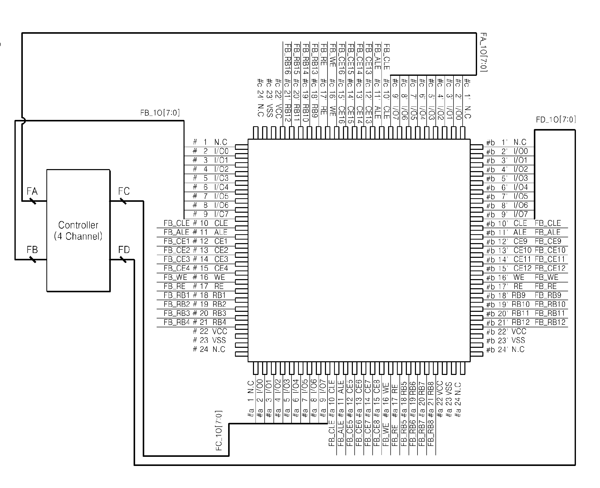
[0047]FIG. 21 is a diagram illustrating eight of the semiconductor packages 100, such a...


PUM


Abstract

Provided is a semiconductor package including multiple semiconductor chips, and separate groups of leads connected to the semiconductor chips. The leads are exposed to the outside of the semiconductor package. The plurality of leads may include a first lead group for a first chip group and a second lead group for a second chip group. The first and second chip groups are part of the package.

Description

CROSS REFERENCE TO RELATED APPLICATIONS[0001]This application claims priority under 35 U.S.C. §119 to Korean Patent Application No. 10-2009-0022747, filed on Mar. 17, 2009, in the Korean Intellectual Property Office, the disclosure of which is incorporated herein by reference in its entirety. This application is also related to co-pending U.S. patent application Ser. No. 12 / 153,558, filed on May 21, 2008, and Korean Patent Application No. 10-2007-0060687, the disclosures of each being incorporated by reference in their entirety.TECHNICAL FIELD OF THE DISCLOSURE[0002]This US patent application relates in general to the art of semiconductor packages, and more particularly, to electrical connections in semiconductor packages having multiple semiconductor chips.BACKGROUND OF THE DISCLOSURE[0003]Semiconductor packages have been continuously developed to have increased integration degree and operating speed and to become thinner, lighter, and smaller. In general, a semiconductor package i...

Claims


Application Information

Patent Timeline
Patent Type & Authority Patents(United States)
IPC IPC(8): H01L23/02
CPCH01L23/49575H01L23/49541H01L25/0657H01L23/535H01L23/50H01L2225/0651H01L24/49H01L2224/48095H01L2224/48145H01L2224/48247H01L2224/4911H01L2224/49175H01L2224/73265H01L2224/83191H01L2225/06562H01L2924/01005H01L2924/01027H01L2924/01075H01L24/48H01L2224/32245H01L2224/32145H01L2924/00014H01L2924/00H01L2924/12042H01L2224/05554H01L2924/181H01L2224/48147H01L2224/45099H01L2224/45015H01L2924/207H01L2924/00012H01L23/12H01L23/48H01L2224/48175
Inventor PARK, CHULKIM, HYSONG-SEOBYEOM, KUN-DAELIM, GWANG-MAN
Owner SAMSUNG ELECTRONICS CO LTD
Features
  • R&D
  • Intellectual Property
  • Life Sciences
  • Materials
  • Tech Scout
  • Unparalleled Data Quality
  • Higher Quality Content
  • 60% Fewer Hallucinations
Learn More