Magnetic sensor

a technology of magnetic sensors and magnetic field, applied in the field of magnetic sensors, can solve the problems of inability to detect high-precision magnetic field, inability to detect differential voltage in the bridge circuit, and errors in the resistance values of respective gmr elements, so as to improve the accuracy suppress variations in resistance values of respective magneto resistive effect elements, and improve the effect of detecting magnetic field

Active Publication Date: 2012-06-05
SAE MAGNETICS (HK) LTD
View PDF3 Cites 16 Cited by
  • Summary
  • Abstract
  • Description
  • Claims
  • Application Information

AI Technical Summary

Benefits of technology

[0014]It is therefore an object of the present invention to provide a magnetic sensor capable of improving accuracy in detecting a magnetic field while realizing size reduction and cost reduction which have been the problems in this field of art.
[0019]According to the present invention, as the bridge circuit is constituted of a plurality of magneto resistive effect elements arranged such that the fixed magnetization direction thereof are in the same direction, the bridge circuit can be formed on a single chip, whereby variations in resistance values of the respective magneto resistive effect elements can be reduced. Further, in the present invention, a magnetic body is arranged in the vicinity of the bridge circuit. With this magnetic body, the direction of the magnetic field existing around the magnetic sensor with respect to the magneto resistive effect elements having the same fixed magnetization direction is changed. Thereby, the external magnetic field in one direction can be changed into different directions between the magneto resistive effect elements, in accordance with the arrangement of the magnetic body. For example, two element forming regions, in each of which a pair of the magneto resistive effect elements not adjacently-connected with each other in the bridge circuit are formed in almost the same area, are provided corresponding to respective pairs of the magneto resistive effect elements, and the magnetic body is arranged such that the magnetic field enters one region in the fixed magnetization direction and enters the other region in the opposite direction. With this configuration, as a large differential voltage can be output from the bridge circuit, accuracy of detecting the magnetic field in one direction can be improved.
[0020]In this case, as the GMR elements constituting the bridge circuit can be formed on a single chip, variations in resistance values thereof can be reduced, so that accuracy of detecting the magnetic field can be improved by suppressing the offset voltage. In addition, as the bridge circuit is formed on a single chip, the size of the chip can be reduced as a whole, whereby the manufacturing efficiency of the chip is improved and the sensor cost can also be reduced.
[0027]According to the present invention which is configured and works as described above, as a large differential voltage is output from the bridge circuit in accordance with a change in the magnetic field in one direction, accuracy of detecting the magnetic field can be improved. In particular, as the bridge circuit can be formed on a single chip, advantages such as variations in resistance values of the respective magneto resistive effect elements are suppressed, accuracy of detecting the magnetic field is improved, and size and costs of the magnetic sensor are reduced, can be achieved.

Problems solved by technology

As such, it is difficult to detect a differential voltage in the bridge circuit.
However, the art disclosed in Non-Patent Document 1 involves a problem that as the resistance values of the two GMR elements, among the GMR elements constituting the bridge circuit, covered with the NiFe film do not vary, a large differential voltage is not output, so that the magnetic field cannot be detected with high accuracy.
However, in the configuration of the GMR elements being separated, a bridge circuit is constituted of a plurality of chips, causing errors in the resistance values of respective GMR elements.
As such, as an offset voltage is caused even when the magnetic field is zero, measurement cannot be performed with high accuracy.
Furthermore, if the bridge circuit is constituted of a plurality of chips, it is necessary to include connecting points, wires, and substrates as described above, causing a problem that the size of the sensor cannot be reduced.
Further, if the offset voltage is large when the magnetic field is zero, the temperature characteristics of the offset voltage deteriorate.
Consequently, a large offset drift is caused, so that it is more difficult to detect the magnetic field with high accuracy.
Further, in the case where the GMR elements are separately provided, they cannot be arranged densely.
Further, when the GMR elements are separately provided, a pad must be formed for each element and the element area becomes larger, so that it is difficult to reduce the size of the chip.
This causes a problem that the number of chips which can be manufactured in the manufacturing steps decreases, so that the product price increases.

Method used


Image

  • Magnetic sensor
  • Magnetic sensor
  • Magnetic sensor

Examples


first embodiment

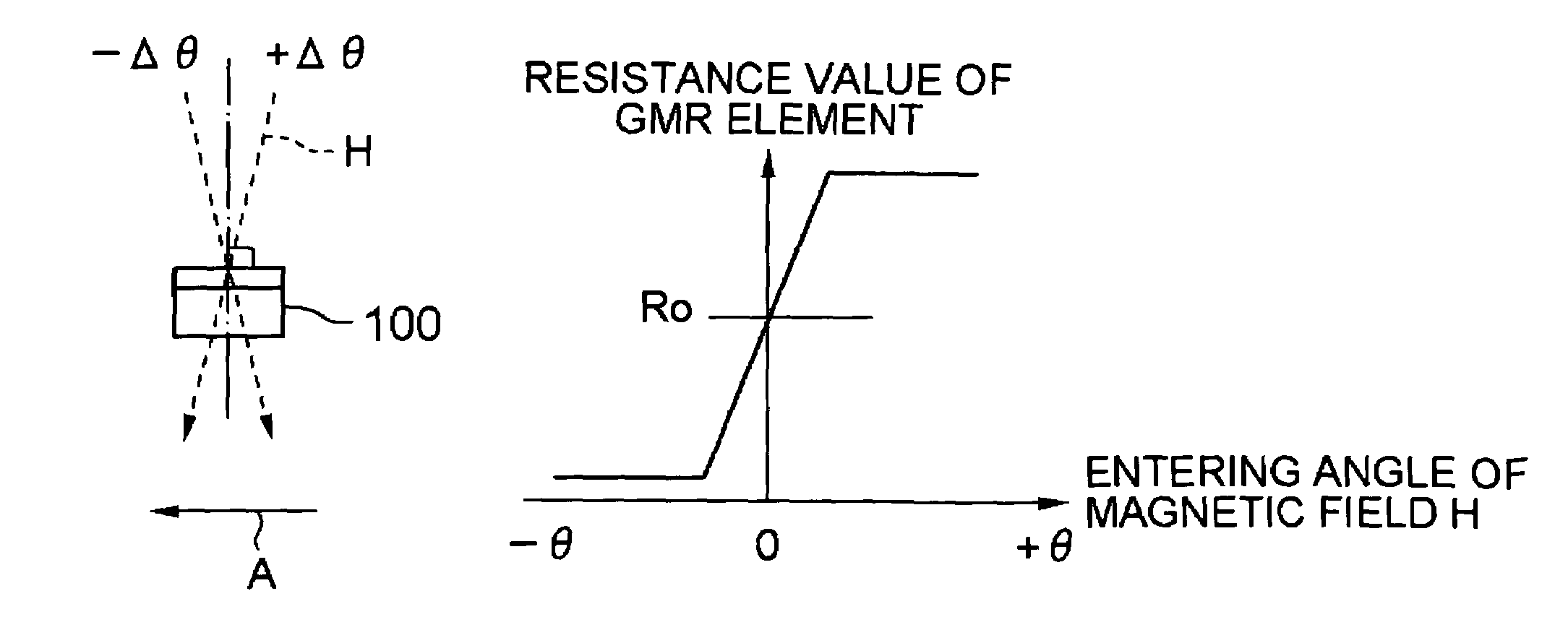
[0044]the present invention will be described with reference to FIGS. 1A to 7. FIGS. 1A and 1B are diagrams illustrating characteristics of a GMR element. FIGS. 2 to 5 show an example of a GMR chip. FIGS. 6 and 7 are diagrams showing an example of a magnetic sensor according to the present embodiment.

[0045]First, characteristics of a GMR element used in the present invention will be described with reference to FIGS. 1A and 1B. The GMR element is a spin-valve type GMR element in which a resistance value to be output varies according to the direction of a magnetic field to be input. FIG. 1A shows a relationship between an entering angle of a magnetic field H relative to the GMR element and a resistance value.

[0046]In the example shown in FIG. 1A, a GMR chip 100 is configured such that GMR elements are formed on the upper surface thereof. These GMR elements are fixedly magnetized in a direction of an arrow A so as to be able to detect a magnetic field in the arrow A direction.

[0047]In ...

second embodiment

[0058]Next, the present invention will be described with reference to FIGS. 8 and 9.

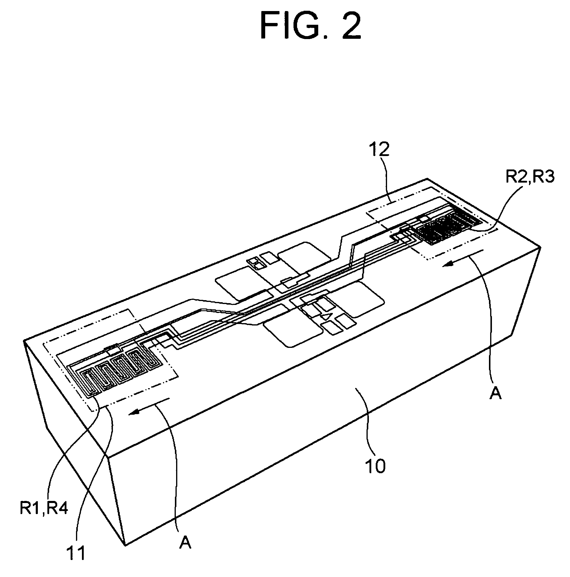
[0059]As shown in FIG. 8, a magnetic sensor 1 of the present embodiment includes two other magnetic bodies 22 and 23 (e.g., soft ferrite (soft magnetic material)), in addition to the magnetic body 21 disposed on the GMR chip 10 in the first embodiment. Specifically, the magnetic bodies 22 and 33 are arranged on both end sides of the GMR chip 10, that is, outside the respective element forming regions 11 and 12. In other words, the magnetic bodies 22 and 23 are respectively arranged at one end of the GMR chip 10 opposite to the element forming region 12 side, and at the other end of the GMR chip 10 opposite to the element forming region 11 side. Thereby, the magnetic bodies 22 and 23 are arranged below the surface on which the GMR elements R1, R2, R3, and R4 are formed in the respective element forming regions 11 and 12.

[Operation]

[0060]Next, operation of the magnetic sensor 1 of the above-described c...

fourth embodiment

[0067]Next, the present invention will be described with reference to FIGS. 12 and 13. In the present embodiment, an ammeter will be described as an example of a measurement device using the magnetic sensor 1.

[0068]As shown in FIG. 12, the ammeter has a magnetic core 3 in an almost square shape (ring shape) in which a part thereof is cut so as to form a gap 30, and the magnetic sensor 1 described in any one of the first to third embodiments is formed in the gap 30. The magnetic sensor 1 is arranged such that the surface on which the GMR elements R1, R2, R3, and R4 are formed faces a cross section of the magnetic core 3 forming the gap 30, that is, one of the opposite walls forming the gap 30, and a conducting wire 31 (conductor) is arranged so as to penetrate almost the center of the magnetic core 3 in an almost square shape as shown in FIG. 13, and electric current flowing through the conducting wire 31 is measured.

[0069]With this configuration, when electric current flows through ...


PUM

PropertyMeasurementUnit
angleaaaaaaaaaa
resistanceaaaaaaaaaa
magnetic fieldaaaaaaaaaa

Abstract

A magnetic sensor capable of detecting a magnetic field with high sensitivity is provided. The magnetic sensor includes a bridge circuit having a plurality of magneto resistive effect elements connected with each other, and is capable of detecting a differential voltage between predetermined connecting points. The magneto resistive effect elements output resistance values which vary in accordance with a direction of a magnetic field to be input, and are arranged such that fixed magnetization directions of all magneto resistive effect elements are in the same direction. Further, a magnetic body which changes the direction of the magnetic field to be input to the magneto resistive effect elements is also provided in the vicinity of the bridge circuit.

Description

BACKGROUND[0001]This application claims priority to Japanese Application No. 2008-126621 filed May 14, 2008, the entire contents of which are hereby incorporated by reference.[0002]1. Technical Field[0003]The present invention relates to magnetic sensors, and in particular, to magnetic sensors using magneto resistive effect elements.[0004]2. Related Art[0005]Magnetic sensors capable of detecting changes in magnetic fields have been developed as measurement devices and used in various applications including ammeters and magnetic encoders. The NVE CORPORATION GMR Sensor Catalog (Non-Patent Document 1) discloses examples of such magnetic sensors, in which GMR (Giant Magneto Resistive effect) elements are used as elements for detecting changes in magnetic fields. A GMR element is an element in which a resistance value to be output varies depending on input magnetism. According to the output resistance value, a detected change in a magnetic field can be measured.[0006]As shown in Non-Pat...

Claims


Application Information

Patent Timeline
Patent Type & Authority Patents(United States)
IPC IPC(8): G01B7/14
CPCG01R33/0005G01R33/09Y10T29/49002
Inventor KASAJIMA, TAMON
Owner SAE MAGNETICS (HK) LTD
Why Eureka
Try Eureka