

Contactless communication medium
a communication medium and contact technology, applied in the direction of semiconductor devices, semiconductor/solid-state device details, instruments, etc., can solve the problems of contact module influence, malfunction or communication disorders of contactless communication medium, and achieve the effect of reducing the possibility of malfunction or communication disorders
- Summary
- Abstract
- Description
- Claims
- Application Information
AI Technical Summary
Benefits of technology
Problems solved by technology
Method used
Image

Examples
example 1
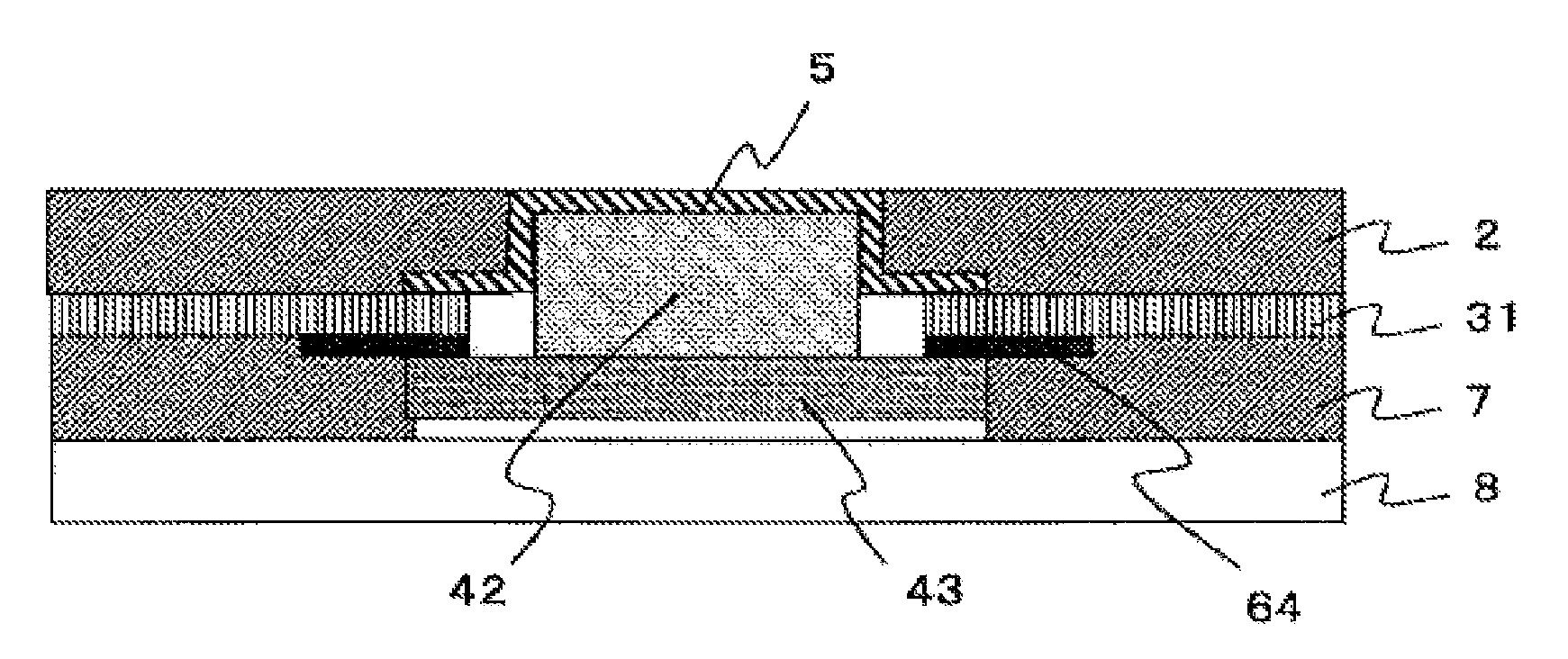
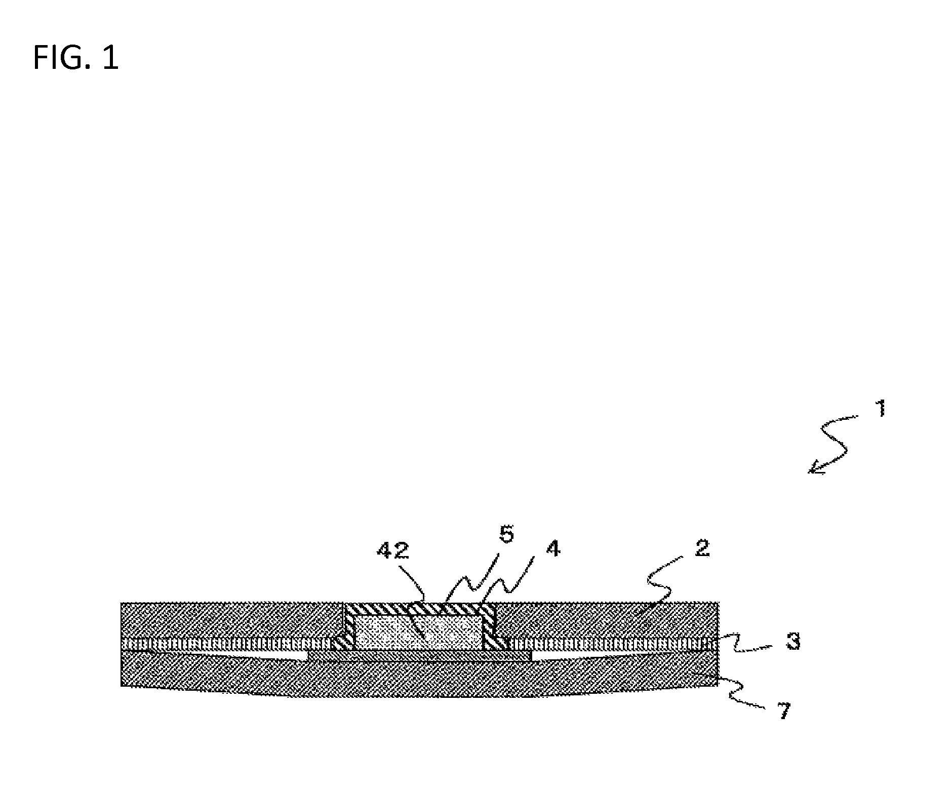
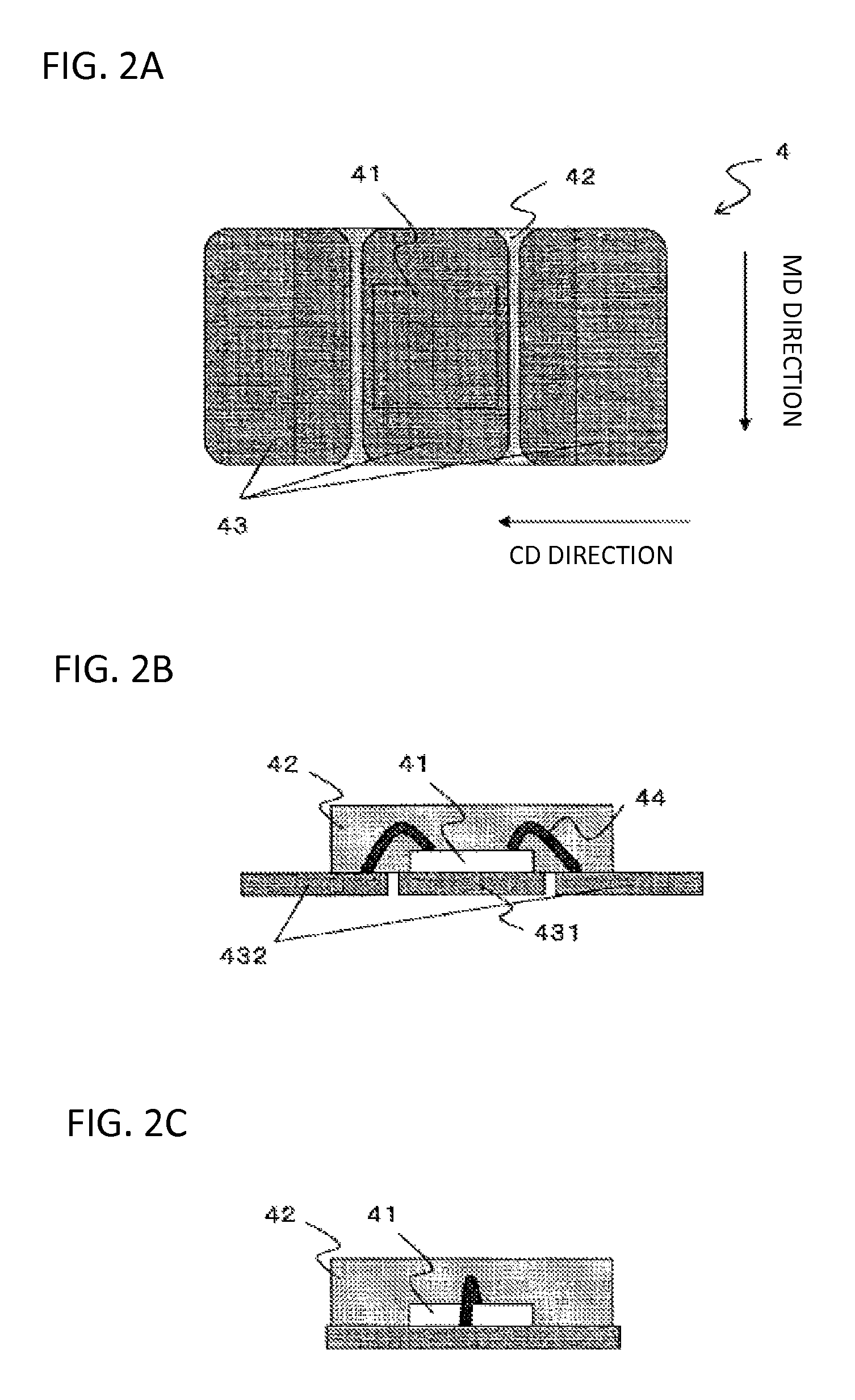
[0096]As the first substrate, polyolefin-based synthetic paper having a thickness of 178 μm and including an opening at a position at which the IC module is to be located is used. As the second substrate, an antenna sheet is used. As the inlay sheet, polyolefin-based synthetic paper having a thickness of 178 μm is used.
[0097]First, an IC module was fit into a hole of the antenna sheet including an antenna and the hole and the IC module was connected to the antenna to obtain an inlet.
[0098]Then, an aqueous emulsion adhesive (EAA) was applied to the first substrate and the inlay sheet, and a sealing member formed of a resin tape was located on the IC module of the inlet so as to cover the mold part. The antenna sheet was held between the first substrate and the inlay sheet such that the IC module and the opening of the first substrate would match each other positionally, and these elements were combined and pressurized to obtain a contactless communication medium. For the sealing memb...
PUM
 Abstract
Description
Claims
Application Information