Electrostatic capacitance detection circuit and input device

a capacitance detection and capacitance detection technology, applied in the direction of resistance/reactance/impedence, pulse technique, instruments, etc., can solve the problems of large influence of noise on output data, inability to ignore the influence of mixture noise, and inability to reduce so as to achieve the effect of greatly improving resistance to external noise and reducing the influence of external nois

Active Publication Date: 2014-02-06
ALPS ALPINE CO LTD
View PDF5 Cites 44 Cited by
  • Summary
  • Abstract
  • Description
  • Claims
  • Application Information

AI Technical Summary

Benefits of technology

[0011]According to the electrostatic capacitance detection circuit, by continuously integrating the electric charge transferred on each of the rising edge and the falling edge of the drive signal in the capacitor, an external noise with a low frequency is averaged, and thus an influence of the external noise can be reduced. Furthermore, because the integral circuit for two systems is not used, the resistance to the external noise can be greatly improved with a minimum circuit configuration.

Problems solved by technology

For this reason, an influence of mixture noise is serious.
Causes of the mixture noise, can be a noise from a power source of a system into which the touch pad and the touch sensor are built, a drive signal of a liquid panel inside the system and others, and an influence of these noise sources cannot be ignored due to the complexity of the apparatus and others.
When a frequency of the noise applied during an integral period is lowered, the averaging of the mixture noise is not sufficient during the integral period, and a larger influence of the noise on output data appears.
In the case of the detect circuit disclosed in U.S. Unexamined Patent Application Publication No. 2011-0273400, the electric charge transfer is performed on both of the edges of the drive pulse and thus the filtering effect on the noise with the low frequency is improved, but an integral circuit, using an operational amplifier, is necessary for two systems, and circuit scale and power consumption are caused to be increased.

Method used


Image

  • Electrostatic capacitance detection circuit and input device
  • Electrostatic capacitance detection circuit and input device
  • Electrostatic capacitance detection circuit and input device

Examples


first embodiment

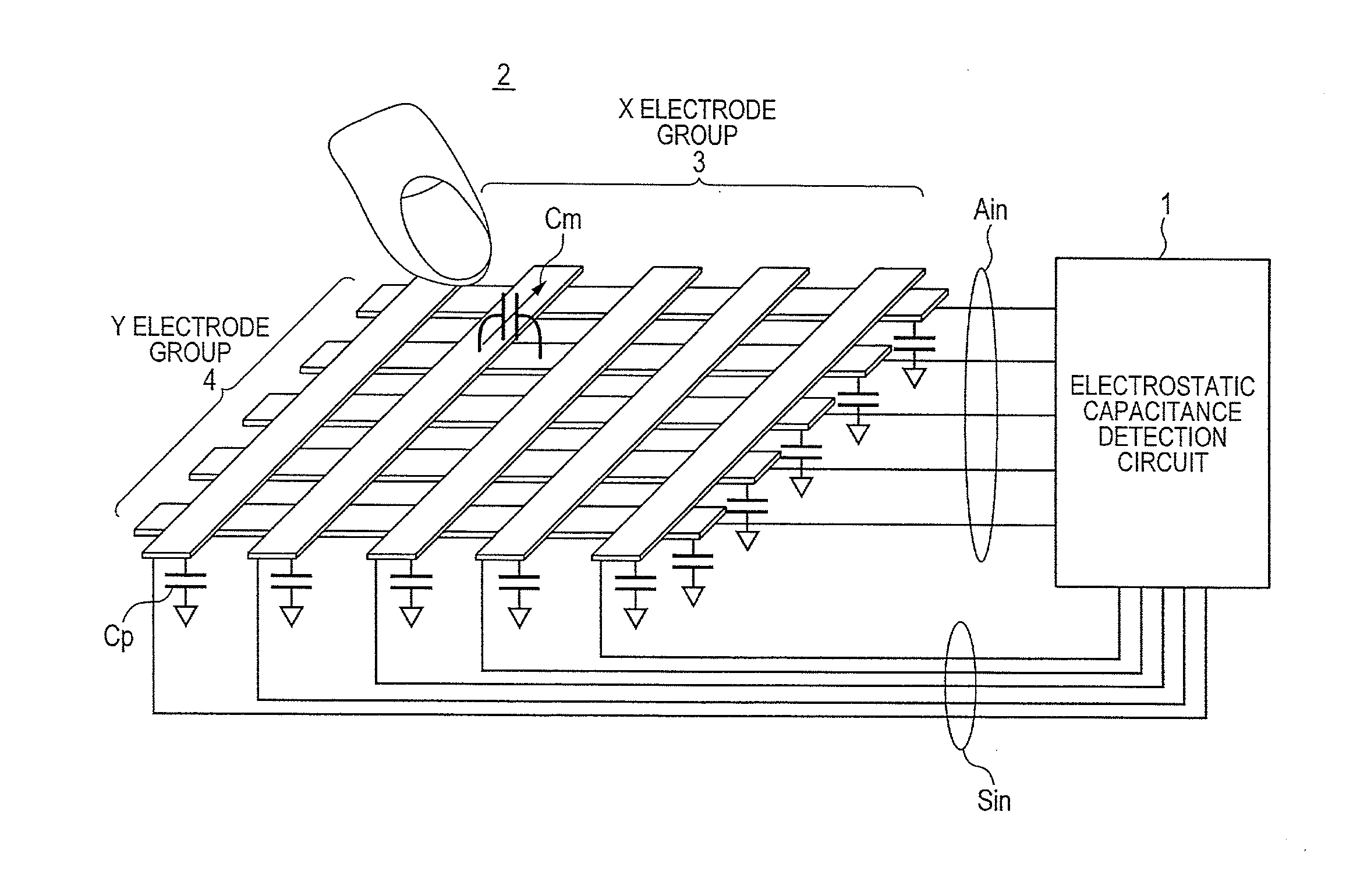
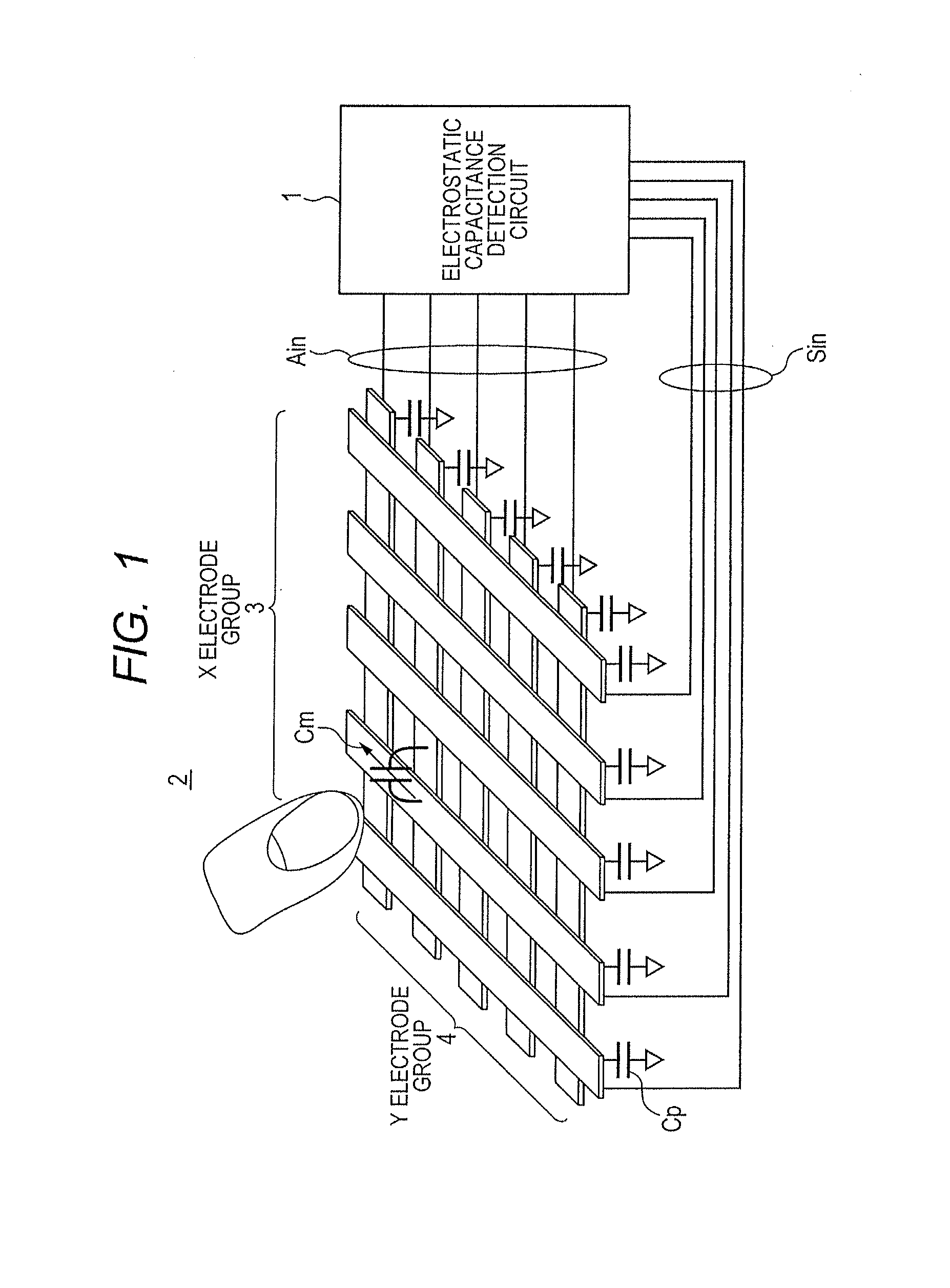
[0038]FIG. 1 illustrates a state in which a sensor electrode 2, such as a touch pad and a touch sensor is connected to an electrostatic capacitance detection circuit 1 according to the first embodiment. The sensor electrode 2 is formed on a two-dimensional plane and an X electrode group 3 and a Y electrode group 4 that intersect each other at right angles are arranged into a matrix form, in the sensor electrode 2. The arrangement of the X electrode group 3 and the Y electrode group 4 of the sensor electrode 2 in a matrix form makes it possible to detect a position that a human finger approaches.

[0039]In each electrode (an X electrode and a Y electrode) of the X electrode group 3 and the Y electrode group 4, a GND capacitor Cp with respect to a sealed substrate is present. Furthermore, an inter-electrode capacitor Cm, although illustrated only in one place in FIG. 1, is formed at each intersection point between the X electrode and the Y electrode. Because the inter-electrode capacito...

second embodiment

[0054]Next, a second embodiment that results from partly modifying the charge amplifier 10 is described.

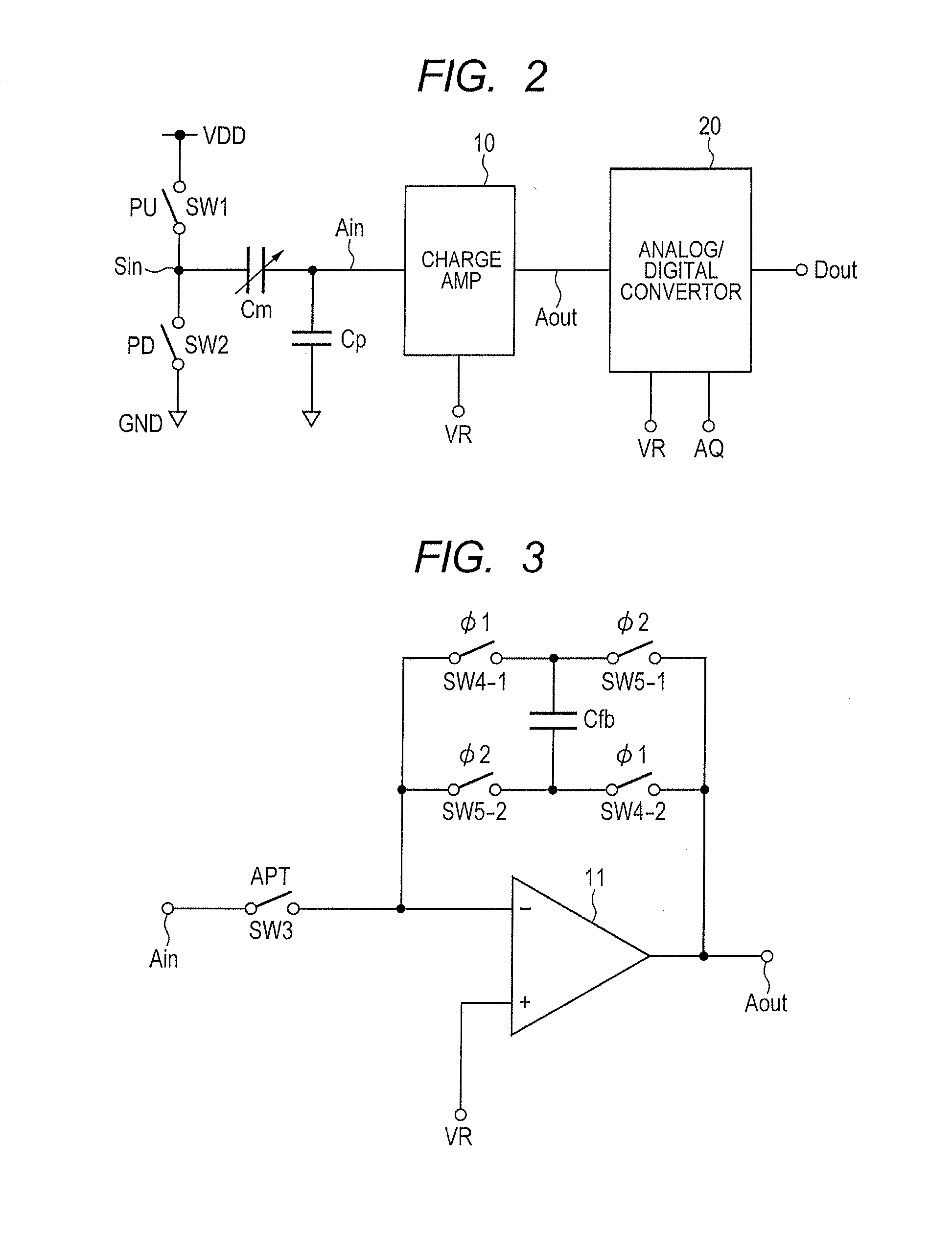
[0055]Because the selection circuit (the selection switches SW4-1, SW5-1, SW4-2, and SW5-2) is controlled with signals φ1 and φ2 is usually controlled in such a manner that the switches are not made ON mutually at the same time, the signals φ1 and φ2 are the non-overlap signals, as illustrated in FIG. 8. Furthermore, in the actual switch, there occurs an electrostatic capacitance coupling between a signal input and output unit through which the data signal is transmitted and is input / output with respect to the switch, and a control signal input unit to which a control signal controlling the switch is input. For example, when working out the design, a technique is employed in which a dummy transistor is provided in order to cancel the coupling thereof, but occasionally influence that cannot be negligible remains. In this case, as illustrated in FIG. 8 and FIG. 9, there is a likelih...

third embodiment

[0058]Next, a third embodiment of the present invention is described. According to the third embodiment, at the time of the rising edge of the drive electrode node Sin, the output Aout is sampled into a sampling capacitor Csn, and at the time of the falling edge of the drive electrode node Sin, the output Aout is sampled into a sampling capacitor Csp.

[0059]FIG. 11 illustrates configurations of the charge amplifier 10 and the analog / digital converter 20 that are applied to the present third embodiment. In FIG. 11, like reference numerals are given to like parts of the charge amplifier 10 illustrated in FIG. 3. The sampling capacitor Csn is connected to a negative input N of the analog / digital converter 20, and the output Aout of the operational amplifier 11 is output through the switch SW4-3 that is controlled with the signal φ1. Furthermore, the sampling capacitor Csp is connected to a positive input P, and the output Aout of the operational amplifier 11 is output through the switch...


PUM


Abstract

An electrostatic capacitance detection circuit includes a charge amplifier that has an operational amplifier in which a capacitor is provided on a feedback path, and into which a signal including detection of electric charge of an inter-electrode capacitor of a sensor electrode and electric charge due to an external noise, and a selection switch that can switch a direction of a capacitor that is connected to input and output terminals of the charge amplifier through a feedback path that switches the direction of the capacitor depending on a direction of electric charge flowing in from a detection-side electrode of the sensor electrode, due to a drive signal applied to the sensor electrode.

Description

CLAIM OF PRIORITY[0001]This application claims benefit of Japanese Patent Application No. 2012-171177 filed on Aug. 1, 2012 and No. 2013-096474 filed on May 1, 2013, which are hereby incorporated by reference in their entireties.BACKGROUND[0002]1. Field of the Disclosure[0003]The present disclosure relates to an electrostatic capacitance detection circuit that detects a minute change in electrostatic capacitance on a sensor such as a touch pad and a touch sensor, and an input device.[0004]2. Description of the Related Art[0005]In the related art, there has been proposed an electrostatic capacitance detection circuit that is suitable for detecting a minute change in electrostatic capacitance between sensor electrodes in an input device such as a touch pad and a touch sensor in a noisy situation.[0006]For example, the electrostatic capacitance detection circuit disclosed in Japanese Patent No. 4275865 employs a configuration in which, to detect mutual capacitance between sensor electr...

Claims


Application Information

Patent Timeline
Patent Type & Authority Applications(United States)
IPC IPC(8): G01R35/00G01R27/26
CPCG01R27/2605G01R35/00G06F3/04182G06F3/0446H03K2217/960725G06F3/0418
Inventor FUJIYOSHI, TATSUMI
Owner ALPS ALPINE CO LTD
Why Eureka
Try Eureka