Concept for compensating the influences of external disturbing quantities on physical functional parameters of integrated circuits

a technology of internal circuits and disturbing quantities, applied in the field of integrated circuits, can solve problems such as mechanical damage of chips, disturbing both effects, and particularly annoying problems

Inactive Publication Date: 2005-06-14
INFINEON TECH AG
View PDF12 Cites 46 Cited by
  • Summary
  • Abstract
  • Description
  • Claims
  • Application Information

AI Technical Summary

Benefits of technology

[0024]In accordance with a first aspect, the present invention provides a circuit for generating an output signal, which depends on a physical useful quantity, having: means for detecting the physical useful quantity, wherein the means for detecting is arranged to generate an output signal, which depends on the physical useful quantity, a control signal for the means for detecting and, with an unchanged control signal, on an external disturbing quantity; sensor means for detecting the external disturbing quantity and for providing a sensor signal, which depends on the external disturbing quantity; and means for processing the sensor signal to influence the control signal dependent on the sensor signal such that the influence of the external disturbing quantity on the output signal is reduced; wherein the circuit further has a memory in which information indicating the influence of the external disturbing quantity on the sensor signal, the control signal and / or the output signal can be stored.
[0025]In accordance with a second aspect, the present invention provides a method for generating an output signal, which depends on a physical useful quantity, having the following steps: detecting the physical useful quantity to generate an output signal which depends on the physical useful quantity, a control signal and, with an unchanged control signal, on an external disturbing quantity; detecting the external disturbing quantity and providing a sensor signal, which depends on the external disturbing quantity; processing the sensor signal to influence the control signal dependent on the sensor signal such that the influence of the external disturbing quantity on the sensor signal, the control signal and / or the output signal is reduced; and storing information indicating the influence of the external disturbing quantity on the output signal.
[0026]The present invention is based on the finding that the influence of an output signal of an integrated circuit by a disturbing quantity, such as, for example, by mechanical stress in the semiconductor material of the integrated circuit, can be decreased or compensated by forming a compensating circuit, such as, for example, a control loop, converting the essential components of the stress tensor acting on the semiconductor material in an on-chip stress sensor into a signal which can be electrical, electronic, thermal, mechanical, etc., wherein this signal is employed to control the integrated circuit, such as, for example, a sensor assembly, in such a way that the output signal of the integrated circuit is influenced selectively so that the influence of the external disturbing quantity, such as, for example, of the mechanical stress in the semiconductor material, on the output signal of the integrated circuit can be decreased considerably or compensated completely.

Problems solved by technology

The problem with influencing physical functional parameters of integrated circuits by external disturbing quantities, such as, for example, by mechanical stress in the semiconductor material of the integrated circuit used, basically occurs in all semiconductor circuits, wherein this problem is found to be particularly annoying in integrated sensors since they use a physical functional parameter of the respective sensor element in order to thereby convert a physical useful quantity to be detected into an electrical output quantity.
Thus, certain disadvantages of indirect semiconductor materials, such as, for example, silicon or germanium, are becoming more and more evident, wherein indirect semiconductor materials are such semiconductors in which the energy maximum of the valence band and the energy minimum of the conducting band are at different crystal impulses.
Both effects are disturbing when operating a sensor assembly, such as, for example, an integrated Hall probe including control and evaluating electronics.
Tensile and compressive stress components occurring in the semiconductor material can easily reach an order of magnitude of 100 MPa(1 Pa=1 N / m2) and can even result in mechanical damage of the chip, i.e. cracks on the surface of the chip or even breaking of the chip.
In particular, mechanical stress in the semiconductor material results in a change of the band structure of the semiconductor.
So far, it has been impossible to keep this mechanical stress in a defined predetermined region during the entire lifetime and the entire temperature range of a sensor assembly.
No gel can be applied to the semiconductor chip supporting the sensor assembly for such thin casing types due to a lack of space, as is otherwise often employed to cast the semiconductor chip with little stress.

Method used


Image

  • Concept for compensating the influences of external disturbing quantities on physical functional parameters of integrated circuits
  • Concept for compensating the influences of external disturbing quantities on physical functional parameters of integrated circuits
  • Concept for compensating the influences of external disturbing quantities on physical functional parameters of integrated circuits

Examples


Embodiment Construction

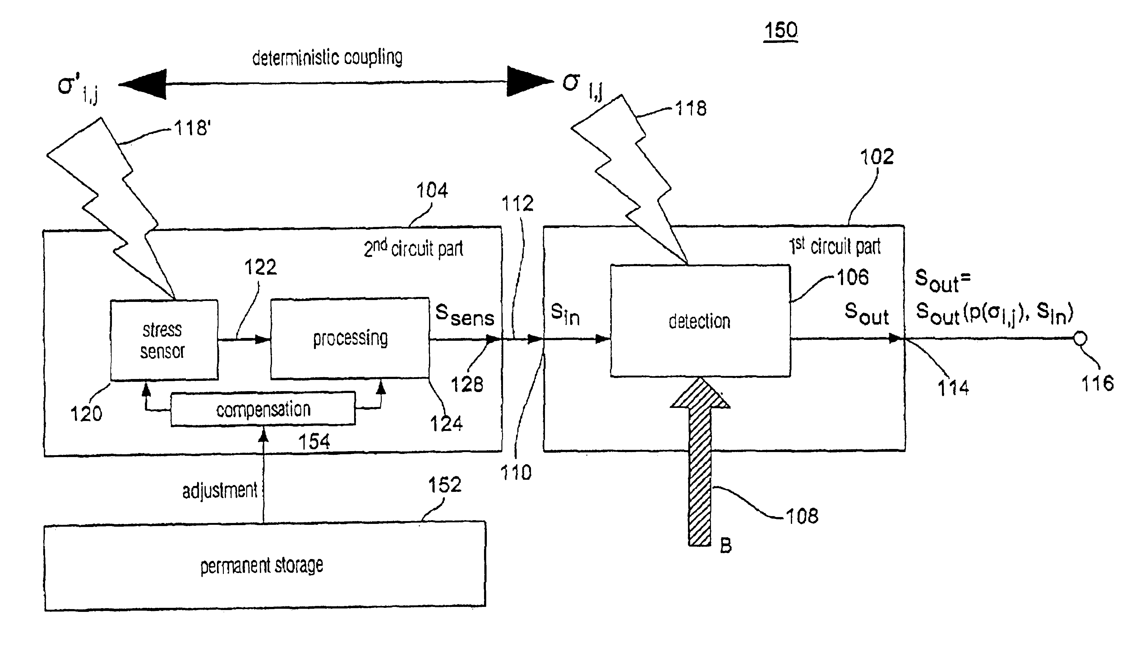
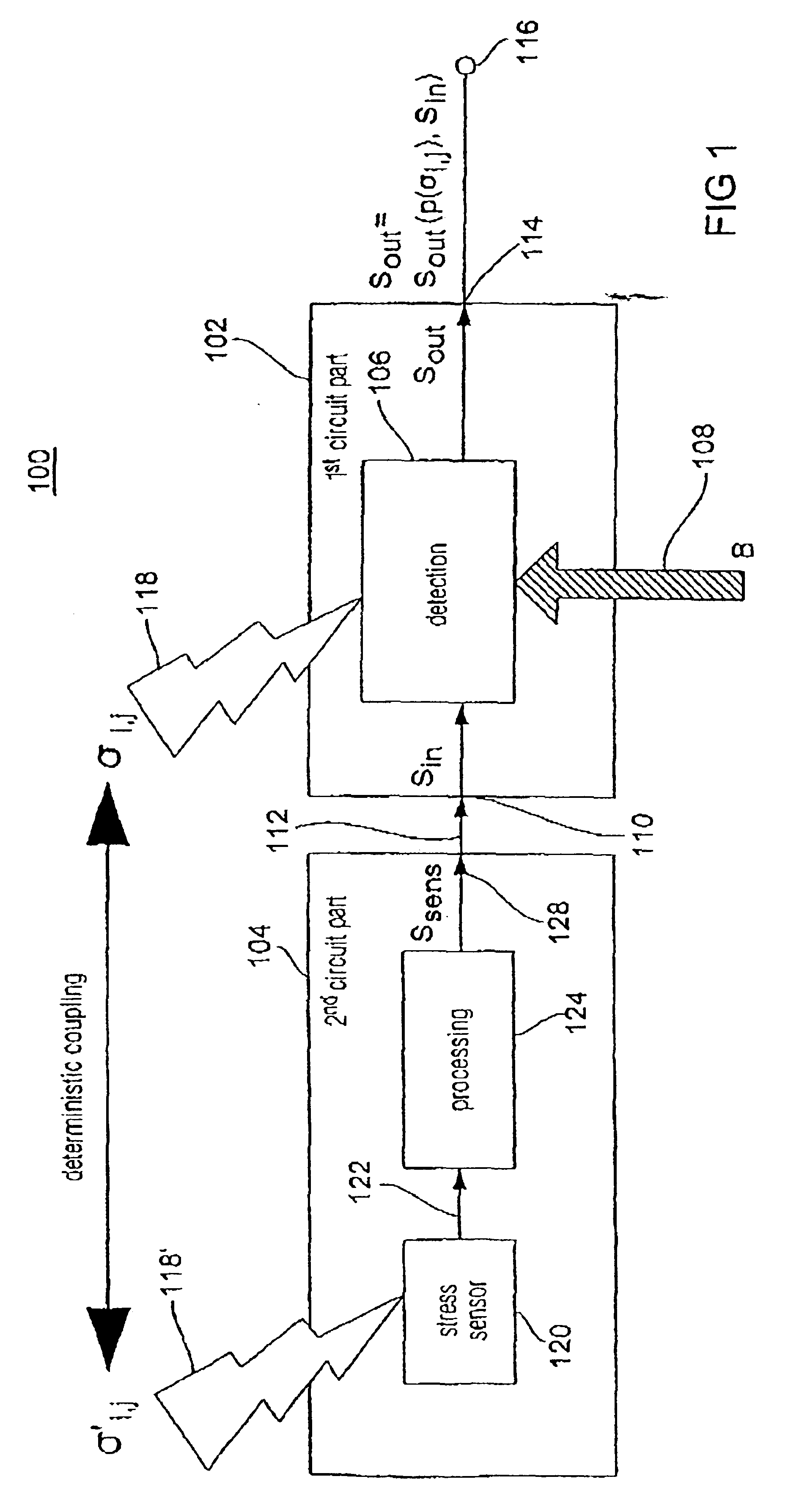
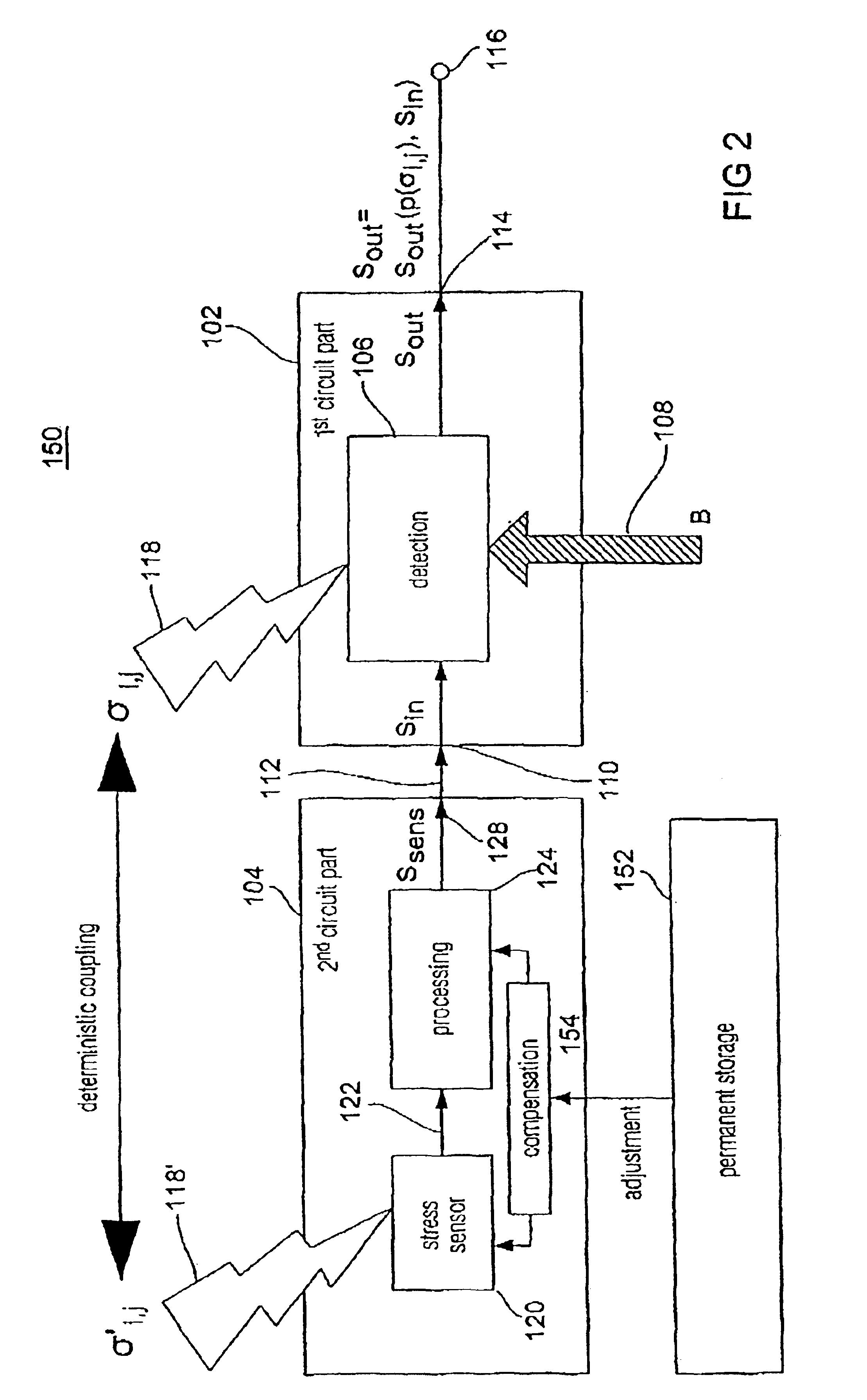
[0043]As regards the general setup of an integrated circuit for generating an output signal independent in relation to external disturbing influences, the signal depending on a physical useful quantity of the integrated circuit, a comparative example will be explained in detail first of all referring to FIG. 1.

[0044]As it is shown in FIG. 1, the integrated circuit 100 comprises a first circuit part 102 and a second circuit part 104. The first circuit part 102 includes means 106 for detecting a physical useful quantity 108 by means of a functional parameter of the means 106 for detecting, wherein the physical useful quantity 108, in the case of a Hall sensor element, is, for example, a magnetic field B to be detected.

[0045]In the context of the present invention, the expression “physical useful quantity” is, however, to be construed in a very general sense since the physical useful quantity can be an electrical, electronic, optical, mechanical, thermal, etc. signal which, for example...


PUM

PropertyMeasurementUnit
compressive stressaaaaaaaaaa
physicalaaaaaaaaaa
mechanical stressaaaaaaaaaa

Abstract

A circuit for generating an output signal, which depends on a physical useful quantity includes means for detecting the physical useful quantity, wherein the means for detecting is arranged to generate an output signal, which depends on the physical useful quantity, a control signal for the means for detecting and, with an unchanged control signal, on an external control quantity. The circuit further includes sensor means for detecting the external disturbing quantity and for providing a sensor signal, which depends on the external disturbing quantity and means for processing the sensor signal to influence the control signal dependent on the sensor signal such that the influence of the external disturbing quantity on the output signal is reduced.

Description

CROSS REFERENCE TO RELATED APPLICATION[0001]This application is a continuation of copending International Application No. PCT / EP02 / 11854, filed Oct. 23, 2002, which designated the United States, and claims priority to German application no. 101 54 495.2 filed Nov. 7, 2001.TECHNICAL FIELD OF THE INVENTION[0002]The present invention relates to integrated circuits and, in particular, to a system concept for decreasing or compensating influences of external disturbing quantities (disturbances), such as, for example, mechanical stress in a semiconductor material, on the physical functional parameters of integrated circuits.DESCRIPTION OF RELATED ART AND BACKGROUND OF THE INVENTION[0003]The problem with influencing physical functional parameters of integrated circuits by external disturbing quantities, such as, for example, by mechanical stress in the semiconductor material of the integrated circuit used, basically occurs in all semiconductor circuits, wherein this problem is found to be ...

Claims


Application Information

Patent Timeline
Patent Type & Authority Patents(United States)
IPC IPC(8): G01D3/036G01D3/028G01R31/28G01R33/06G01R33/07G01R35/00H01H79/00H01L23/58H04B15/00H04B1/10G01L1/26G06F
CPCG01L1/26G01D3/0365
Inventor AUSSERLECHNER, UDO
Owner INFINEON TECH AG
Why Eureka
Try Eureka