Solid-state image capturing apparatus, driving method of a solid-state image capturing apparatus, and electronic information device

a solid-state image and capturing apparatus technology, applied in the direction of color television details, television system details, television system, etc., can solve the problems of deterioration of the picture quality of dark images, in particular, the chip size is large, and the dynamic range of captured images is wide. , to achieve the effect of widening the dynamic range of captured images

Active Publication Date: 2012-08-14
SMARTSENS TECH (SHANGHAI) CO LTD
View PDF9 Cites 9 Cited by
  • Summary
  • Abstract
  • Description
  • Claims
  • Application Information

AI Technical Summary

Benefits of technology

[0019]The present invention is intended to solve the conventional problems described above. The objective of the present invention is to provide a solid-state image capturing apparatus, which avoids using a field memory that causes the increase in the chip size, and further avoids the influence of leak current to a data signal to be sample-held, while widening the dynamic range of a captured image; a driving method for the solid-state image capturing apparatus; and an electronic information device having the solid-state image capturing apparatus used therein.
[0069]According to the present invention with the structure described above, a solid-state image capturing apparatus includes: a pixel area in which pixels for generating a signal charge by a photoelectric conversion on an incident light are arranged in two dimensional matrix; and a row selection section for selecting each pixel row of the pixel area, the solid-state image capturing apparatus successively outputting a pixel value of each pixel of a pixel row selected by the row selection section. The solid-state image capturing apparatus further includes a plurality of column signal lines, to which an analog pixel signal from each pixel of the pixel row selected by the row selection section is read out, the column signal lines being provided for each pixel column in the pixel area, and a signal processing circuit for generating a digital pixel value from the analog pixel signal of each pixel that is read out to each of the column signal lines. Further, the signal processing circuit includes at least two or more AD conversion circuits for simultaneously converting the analog pixel signal of each pixel of the selected pixel row that is read out to each of the plurality of column signal lines into a digital pixel value. Thus, it becomes possible to read out a long time exposure analog pixel signal, which corresponds to a signal charge obtained by long time exposure, and a short time exposure analog pixel signal, which corresponds to a signal charge obtained by short time exposure, to a column signal line that corresponds to each pixel to simultaneously AD converts the long time exposure analog pixel signal and the short time exposure analog pixel signal into respective digital pixel values. As a result, the digital pixel values of the long time exposure analog pixel signal and the short time exposure analog pixel signal are combined, thereby enabling to avoid using a field memory that causes the increase in the chip size, and avoid the influence of leak current to a data signal to be sample-held, while widening the dynamic range of a captured image.

Problems solved by technology

The CMOS image sensor disclosed in Reference 1 described above has a problem with the chip size becoming large since a field memory is used to achieve the wide dynamic range in a captured image.
Due to this, a problem exists in which the picture quality of a dark image, in particular, is deteriorated by the influence of leak current and the like.
This problem occurs because the sample hold CDS circuit includes a switch transistor and a capacitor and therefore the amount of attenuation, in which the sample-held data signal is attenuated by the leak current in the transistor, varies depending on the length of the time for the sample holding.

Method used


Image

  • Solid-state image capturing apparatus, driving method of a solid-state image capturing apparatus, and electronic information device
  • Solid-state image capturing apparatus, driving method of a solid-state image capturing apparatus, and electronic information device
  • Solid-state image capturing apparatus, driving method of a solid-state image capturing apparatus, and electronic information device

Examples


embodiment 1

[0118](Embodiment 1)

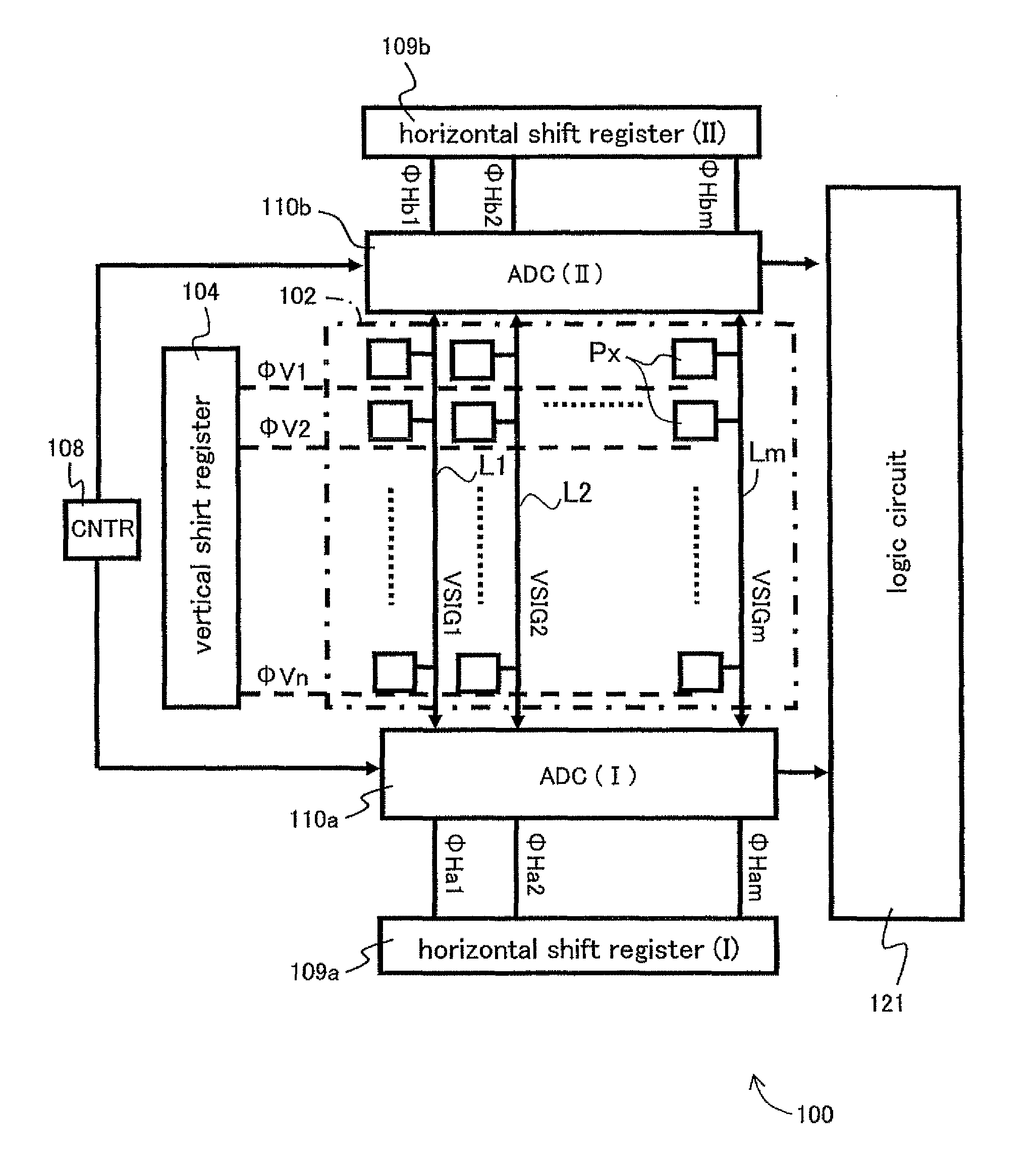
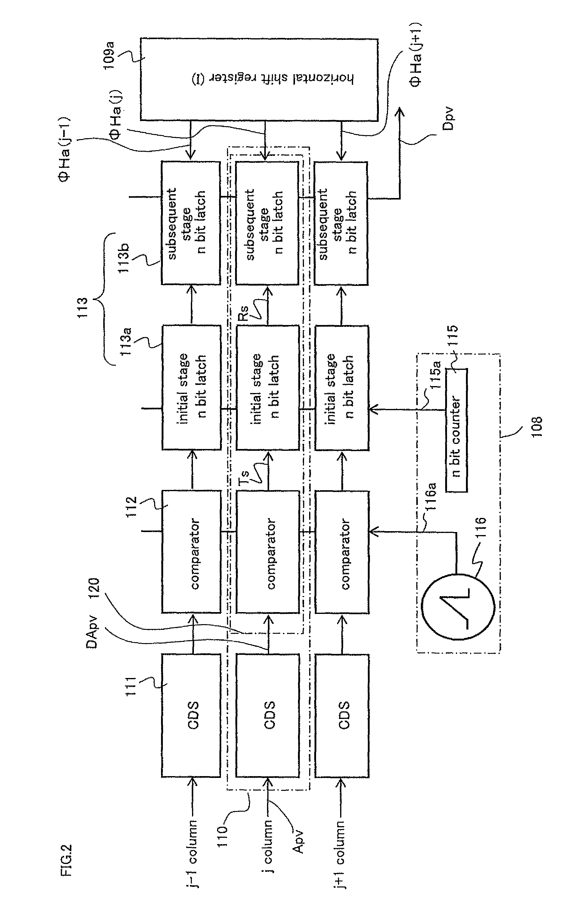
[0119]FIGS. 1 to 6 are diagrams describing a solid-state image capturing apparatus according to Embodiment 1 of the present invention and a driving method of the solid-state image capturing apparatus. FIG. 1 is a block diagram illustrating the configuration of the solid-state image capturing apparatus according to Embodiment 1. FIG. 2 is a block diagram describing an AD conversion circuit in the solid-state image capturing apparatus. FIGS. 3 and 4 are each a waveform diagram describing an operation of the solid-state image capturing apparatus according to Embodiment 1. FIG. 3 illustrates timing of occurrence of row selection pulses within one frame period. FIG. 4(a) illustrates timing of occurrence of row selection pulses within one horizontal period. FIGS. 4(b) and 4(c) respectively illustrate timing of occurrence of column selection pulses that are outputted from first and second horizontal shift registers. FIG. 5 is a diagram illustrating timing of long time e...

embodiment 2

[0168](Embodiment 2)

[0169]Hereinafter, a specific description will be given with regard to a solid-state image capturing apparatus according to Embodiment 2 for performing feedback control on the maximum amplitude value of a ramp waveform supplied to the first and second AD conversion circuits described above.

[0170]FIGS. 7 and 8 are each a diagram describing a solid-state image capturing apparatus according to Embodiment 2 of the present invention. FIG. 7 illustrates an overall configuration of the solid-state image capturing apparatus according to Embodiment 2, and FIG. 8 illustrates the configuration of an AD conversion circuit and its control section for an analog pixel signal in the solid-state image capturing apparatus.

[0171]Instead of the control section 108 of the solid-state image capturing apparatus 100 according to Embodiment 1 described above, the solid-state image capturing apparatus according to Embodiment 2 includes a control section 108a. The control section 108a incl...

embodiment 3

[0176](Embodiment 3)

[0177]FIGS. 9 to 12 are each a diagram describing a solid-state image capturing apparatus according to Embodiment 3 and a method for driving the solid-state image capturing apparatus. FIG. 9 is a block diagram illustrating the configuration of the solid-state image capturing apparatus according to Embodiment 3. FIG. 10 is a schematic view describing the operation of the solid-state image capturing apparatus according to Embodiment 3. FIGS. 11 and 12 are each a waveform diagram describing the operation of the solid-state image capturing apparatus according to Embodiment 3. FIG. 11 is a diagram illustrating the timing of occurrence of row selection pulses within one frame period. FIG. 12(a) is a diagram illustrating the timing of occurrence of row selection pulses within one horizontal period. FIGS. 12(b) and 12(c) are respectively diagrams illustrating the timing of occurrence of column selection pulses outputted from first and second horizontal shift registers.

[0...


PUM


Abstract

A solid-state image capturing apparatus according to the present invention includes a pixel area in which pixels for generating a signal charge by a photoelectric conversion on an incident light are arranged in a two dimensional matrix; a row selection section for selecting each pixel row of the pixel area; a plurality of column signal lines, to which an analog pixel signal from each pixel of a pixel row selected by the row selection section is readout; and a signal processing circuit for generating a digital pixel value from the analog pixel signal of each pixel that is read out to each of the column signal lines, where the signal processing circuit includes at least two or more AD conversion circuits for simultaneously converting the analog pixel signal of each pixel of the selected pixel row into a digital pixel value.

Description

[0001]This nonprovisional application claims priority under 35 U.S.C. §119(a) to Patent Application No. 2008-141709 filed in Japan on May 29, 2008, the entire contents of which are hereby incorporated by reference.BACKGROUND OF THE INVENTION[0002]1. Field of the Invention[0003]The present invention relates to a solid-state image capturing apparatus, a driving method of the solid-state image capturing apparatus, and an electronic information device, and in particular to a solid-state image capturing apparatus for performing a pixel row selecting operation to obtain an image signal with a wide dynamic range, using a short time exposure and a long time exposure, a driving method of the solid-state image capturing apparatus, and an electronic information device having the solid-state image capturing apparatus used therein.[0004]2. Description of the Related Art[0005]While CCD image sensors and CMOS image sensors are conventionally used for image capturing apparatuses, for outputting an ...

Claims


Application Information

Patent Timeline
Patent Type & Authority Patents(United States)
IPC IPC(8): H04N5/335H04N5/341H04N5/353H04N5/355H04N5/357H04N5/361H04N5/363H04N5/374H04N5/378
CPCH04N5/35554H04N5/378H04N25/583H04N25/75
Inventor SHOHO, MAKOTOHASHIGUCHI, KAZUO
Owner SMARTSENS TECH (SHANGHAI) CO LTD
Why Eureka
Try Eureka