Semiconductor memory device for high-speed data input/output

a memory device and high-speed technology, applied in the direction of information storage, static storage, digital storage, etc., can solve the problems of difficult serialization of data within a time period, and the structure is not applicable to a semiconductor memory device that operates at a high speed, so as to achieve high speed and increase the reliability of operation

Active Publication Date: 2012-08-14
SK HYNIX INC
View PDF15 Cites 4 Cited by
  • Summary
  • Abstract
  • Description
  • Claims
  • Application Information

AI Technical Summary

Benefits of technology

[0017]Embodiments of the present invention are directed to increasing the reliability of an operation of a semiconductor memory device, which operates at a high speed, by aligning output data stably. A long operation margin is secured for alignment of internal data, thereby dealing with a high-frequency system clock.
[0018]Embodiments of the present invention are also directed to increasing the reliability of an operation of a semiconductor memory device, which operates at a high speed, by aligning output data stably. A preamble data pattern is selectively output to internal data, thereby preventing a data distortion (delay or skew) that may occur during the data input / output operation.
[0019]A semiconductor memory device requiring a high-speed operation must be able to input / output more data within a short time in response to a system clock. To this end, a semiconductor memory device in accordance with an embodiment of the present invention outputs internal parallel data corresponding to a read operation 1.5 tCK earlier than a data output time point, and secures a sufficient operation margin for serialization for output through an input / output pad. Also, a data output circuit in the semiconductor memory device performs a step-by-step serialization operation by using a plurality of multiplexers, a plurality of latch units, and a plurality of phase shifters that make it possible to serialize data input in parallel within an operation margin of 1.5 tCK and to output data at a time point of a CAS latency CL after application of a read command. The data output circuit of the present invention converts 8-bit parallel input data into four parallel data of 2-bit serial data, converts the four parallel data into two parallel data of 4-bit serial data, and finally converts the two parallel data into 8-bit serial data. Therefore, a sufficient operation margin for data alignment can be secured, thus making it possible for the semiconductor memory device to output aligned data in response to a system clock with a higher frequency.

Problems solved by technology

However, the semiconductor memory device is required to operate according to a system clock with a higher frequency, and it is difficult to serialize data within a time period shorter than 0.5 ns, when considering an operation margin of a 4:1 multiplexer MUX used as the first multiplexer 120 and the second multiplexer 140 illustrated in FIG. 1.
Thus, the semiconductor memory device using the data output circuit illustrated in FIG. 1 has no choice but to have the limit of an operation frequency, and such a structure is not applicable to a semiconductor memory device that operates at a high speed.

Method used


Image

  • Semiconductor memory device for high-speed data input/output
  • Semiconductor memory device for high-speed data input/output
  • Semiconductor memory device for high-speed data input/output

Examples


Embodiment Construction

[0039]Hereinafter, a semiconductor memory device for high-speed data input / output in accordance with the present invention will be described in detail with reference to the accompanying drawings.

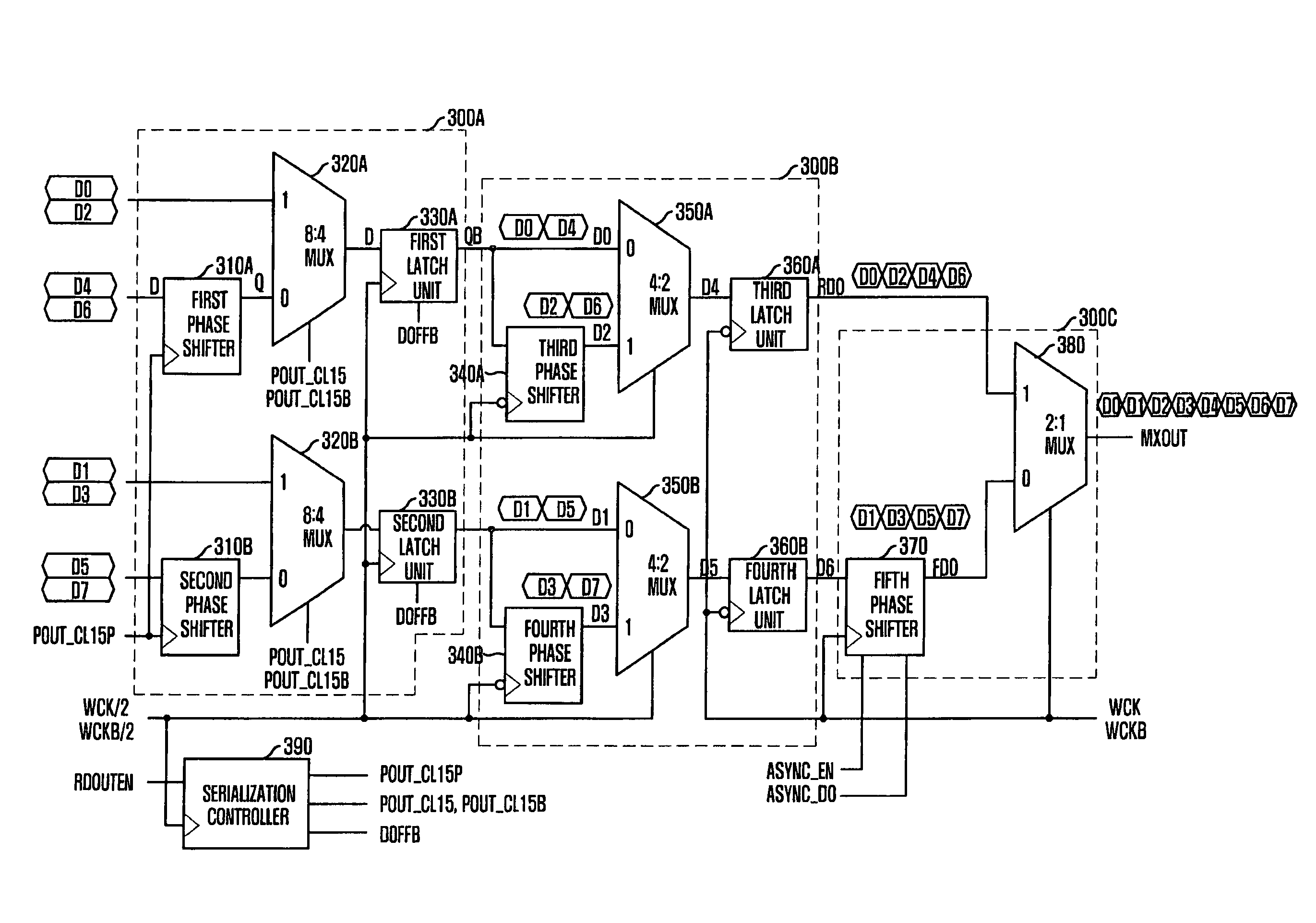
[0040]FIG. 3 is a block diagram of a data output circuit of a semiconductor memory device in accordance with an embodiment of the present invention.

[0041]Referring to FIG. 3, the data output circuit includes a first serializer 300A, a second serializer 300B, and a third serializer 300C. The first serializer 300A is configured to serialize input 8-bit parallel data to output first to fourth 2-bit serial data. The second serializer 300B is configured to receive the output of the first serializer 300A to output fifth and sixth 4-bit serial data. The third serializer 300C is configured to receive the output of the second serializer 300B to output seventh 8-bit serial data.

[0042]Herein, the first serializer 300A includes first and second phase shifters 310A and 310B, first and second multiplexers...


PUM


Abstract

Semiconductor memory device for high-speed data input / output includes a first serializer configured to partially serialize input 8-bit parallel data to output first to fourth serial data, a second serializer configured to partially serialize the first to fourth serial data to output fifth and sixth serial data and a third serializer configured to serialize the fifth and sixth serial data to output seventh serial data.

Description

CROSS-REFERENCE TO RELATED APPLICATIONS[0001]The present invention claims priority of Korean patent application number 10-2008-0019064 and 10-2008-0019065 filed on Feb. 29, 2008, respectively which is incorporated by reference in their entirety.BACKGROUND OF THE INVENTION[0002]The present invention relates to a semiconductor memory device capable of operating at a high speed, and more particularly, to a data output control circuit for aligning and controlling a plurality of data output from a semiconductor memory device that operates at a high speed.[0003]In a system with a variety of semiconductor devices, a semiconductor memory device serves as a data storage unit. The semiconductor memory device outputs data corresponding to addresses received from a data processor, e.g., a central processing unit (CPU), or stores data received from the data processor into memory cells selected by addresses.[0004]As the operating speed of the system increases and semiconductor integrated circuit ...

Claims


Application Information

Patent Timeline
Patent Type & Authority Patents(United States)
IPC IPC(8): G11C7/00
CPCG11C7/1006G11C7/1012G11C7/1018G11C7/1051G11C7/1078G11C2207/107
Inventor SHIN, BEOM-JUYOON, SANG-SIC
Owner SK HYNIX INC
Why Eureka
Try Eureka