
Liquid crystal display device

Active Publication Date: 2012-08-28
LG DISPLAY CO LTD
View PDF11 Cites 3 Cited by
  • Summary
  • Abstract
  • Description
  • Claims
  • Application Information

AI Technical Summary

Benefits of technology

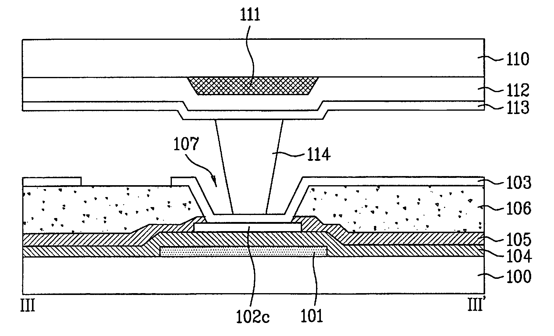
[0026]Accordingly, an LCD device is provided which can obviate one or more problems of the related art. In particular, an LCD device according to the present invention includes first and second substrates facing each other, whereby crossing gate and data lines are formed on the first substrate to define a pixel region. A thin film transistor is provided that includes a gate electrode protruding from the gate line, a source electrode protruding from the data line and a drain electrode spaced from the source electrode at a predetermined interval. A metal pattern is disposed over a predetermined portion of the gate line. A passivation layer is disposed over the data line and the metal pattern, the passivation layer having a contact hole exposing the drain electrode and a storage hole exposing the metal pattern. A pixel electrode is disposed on the pixel region over the contact hole and the storage hole. A column spacer is configured to contact the pixel electrode through the storage hole. A liquid crystal layer is interposed between the first and second substrates. The LCD device may further include a color filter layer and black matrix layer formed on either of the substrates.

Problems solved by technology

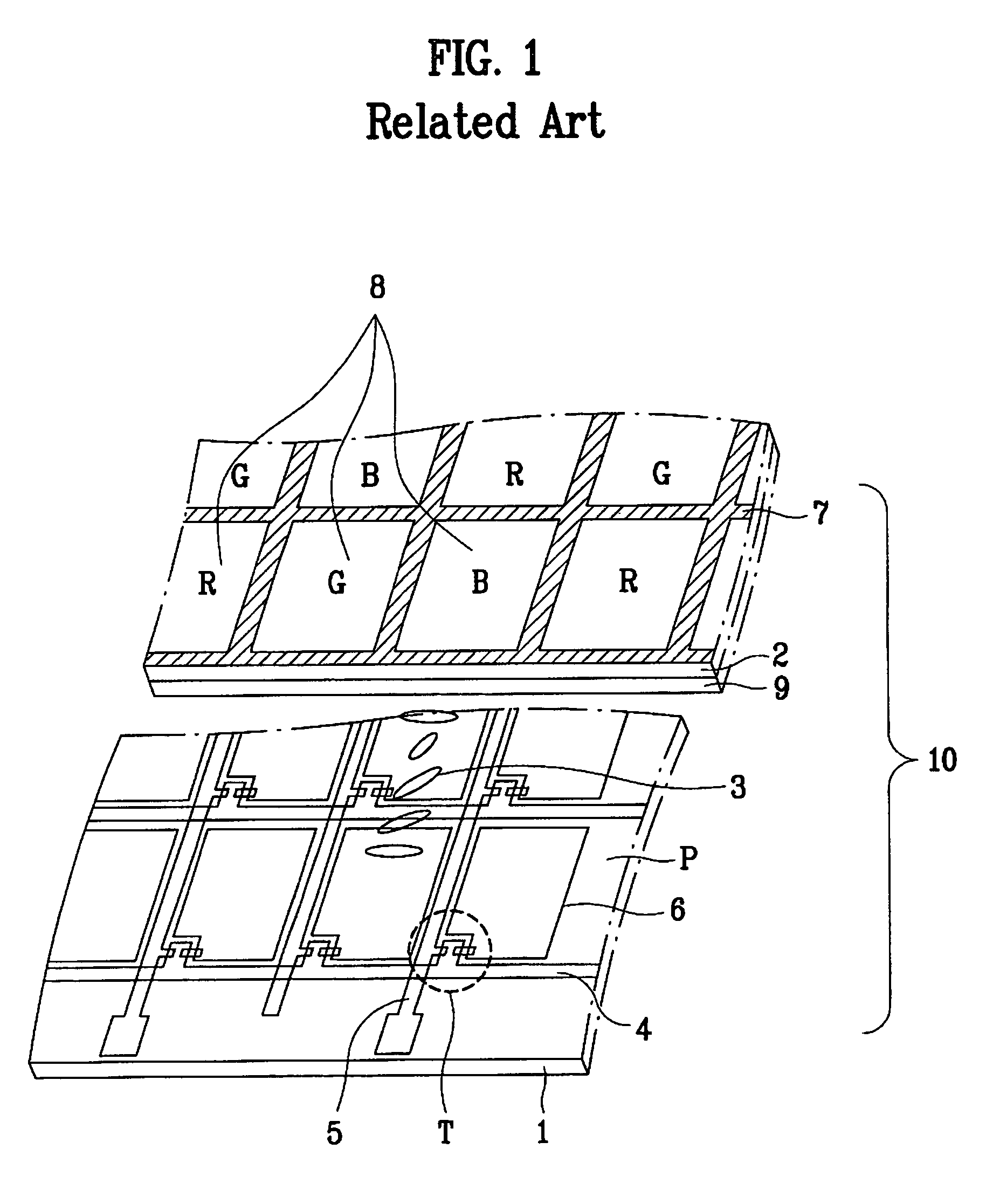
The above-described twisted nematic (TN) mode LCD device has a characteristic disadvantage of narrow viewing angles.
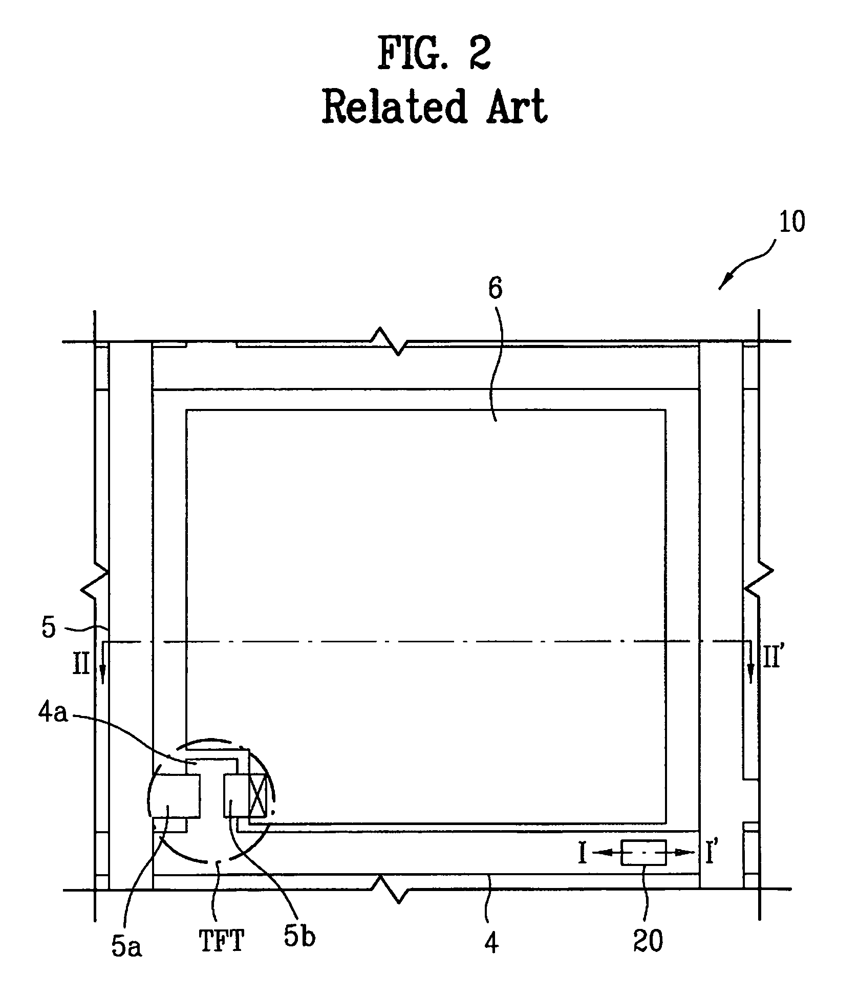
This touch defect is caused by frictional forces generated by the large contact areas between the column spacer and its opposing lower substrate.
Consequently, a peripheral portion of the data line 5 that was formerly covered by the black matrix layer 7 before touching becomes exposed after touching, thereby resulting in leakage of light.

Method used


Image

  • Liquid crystal display device
  • Liquid crystal display device
  • Liquid crystal display device

Examples


Embodiment Construction

[0040]Reference will now be made in detail to the preferred embodiments of the present invention, examples of which are illustrated in the accompanying drawings. FIG. 7 is a plane view illustrating an LCD device according to one embodiment of the present invention FIG. 8 is a sectional view taken along line III˜III′ of FIG. 7. The LCD device includes a first substrate 100 having a thin film transistor array, a second substrate 110 having a color filter array, and a liquid crystal layer (not shown) between the first and second substrates 100 and 110. The first and second substrates 100 and 110 face each other.

[0041]The first substrate 100 includes gate and data lines 101 and 102 crossing each other to define a pixel region, a gate insulating layer 104 formed between the gate and data lines 102, and a thin film transistor TFT (FIG. 7). The TFT includes a gate electrode 101a protruding from the gate line 101, a source electrode 102a protruding from the data line 102 and a drain electro...


PUM


Abstract

An LCD device according to the present invention includes having first and second substrates facing each other gate and data lines crossing each other to define a pixel region, a thin film transistor including a gate electrode protruding from the gate line, a source electrode protruding from the data line and a drain electrode spaced from the source electrode at a predetermined interval, a metal pattern over a predetermined portion of the gate line, a passivation layer over the data line and the metal pattern to have a contact hole exposing the drain electrode and a storage hole exposing the metal pattern, a pixel electrode on the pixel region over the contact hole and the storage hole, a column spacer contacting with the pixel electrode through the storage hole and a liquid crystal layer between the first and second substrates.

Description

[0001]This application claims the benefit of priority to Korean Patent Application No. P2005-29408, filed on Apr. 8, 2005, herein incorporated by reference.TECHNICAL FIELD[0002]The present invention relates to a liquid crystal display (LCD) device, and more particularly, to an LCD device in which a column spacer is configured to contact a storage hole to minimize movement of substrates due to external forces such as touch.BACKGROUND[0003]With the development of an information-based society, the demand for display devices has increased. Accordingly, there has been significant research and development of various flat display devices, including liquid crystal display (LCD), plasma display panel (PDP), electroluminescent display (ELD), and vacuum fluorescent display (VFD) devices. Some of these flat display devices have already been applied to displays in various devices.[0004]Among the various flat display devices, the liquid crystal display (LCD) device has been widely used due to its...

Claims


Application Information

Patent Timeline
IPC IPC(8): G02F1/1339G02F1/1333G02F1/136
CPCG02F1/13394G02F1/133512G02F1/136227H01L27/1214H01L27/13B60Q1/28B60Q1/44B60Y2200/11
Inventor PARK, SEUNG RYULLLEE, JOON DONG
Owner LG DISPLAY CO LTD
Learn More