High-voltage semiconductor device

a semiconductor device and high-voltage technology, applied in semiconductor devices, diodes, electrical devices, etc., can solve the problems of increasing severe electric field on the surface of high-voltage semiconductor devices, and thick dielectric layer tox, so as to reduce the cost of soi substrates. , the effect of reducing the warping of wafers in the manufacturing process

Active Publication Date: 2012-09-18
FUJI ELECTRIC CO LTD
View PDF12 Cites 6 Cited by
  • Summary
  • Abstract
  • Description
  • Claims
  • Application Information

AI Technical Summary

Benefits of technology

[0036]In view of the above problems, it is an object of embodiments of the present invention to provide a high-voltage semiconductor device in which an elevated withstand voltage is achieved at a low cost for a level shifter element of a high withstand voltage NMOSFET formed on an SOI substrate without any complicated manufacturing process such as addition of back surface steps. Another object of embodiments of the invention is to provide a high-voltage semiconductor device that achieves low voltage driving and quick response, owing to stable high voltage wiring and a low ON voltage.
[0047]The high-voltage semiconductor device of embodiments of the invention allows a thickness of the embedded dielectric layer required for achieving a predetermined withstand voltage minimized. Thus, a high withstand NMOSFET is attained at a low substrate cost. Since a thick embedded dielectric layer, like in the single stage structure, is not required, the problem of warping of wafer in the manufacturing process is minimized.
[0048]Since a plurality of stages of concentric transistors are formed so that the drain of each transistor is surrounded by the source, despite wiring connection between the drain of a low potential side transistor and the source of the adjacent high potential side transistor, no potential difference exists between the drain and the source. Thus, generation of leakage current is suppressed between the source and the drain. As a result, ignoring the leakage current and dielectric breakdown of an oxide film, a voltage born by one transistor can be increased. High voltage born by one transistor leads to reduction of the number of stages of series connected transistors. Consequently, the capacitance component is reduced in the level shift circuit section including the high withstand voltage NMOSFETs and in addition, low ON voltage operation can be performed. Therefore, the turn ON / OFF transfer delay time of the whole high side driving circuit is shortened, to provide a high-voltage semiconductor device performing fast response. The number of stages is reduced from the construction disclosed in Patent Document 3, described above. Therefore, a range of scattering in ON current is reduced for the entire level shifter element with a series connected multiple stage construction, implementing stable switching operation.

Problems solved by technology

The thickness Tox of the dielectric layer 901 also has a problem of rise of an SOI substrate cost because of a problem of large warp of the wafer in the IC production process for a thick SOI substrate with a laminated construction and because of increase in deposition time of dielectric layer 901 using a high temperature furnace.
Thus, an electric field on the surface of the high-voltage semiconductor device becomes severe and the withstand voltage decreases.
Consequently, reality in mass production is lost in an SOI substrate with a dielectric layer composed of a silicon oxide film having a thickness not smaller than Tox=6 μm, in consideration of a withstand voltage, a substrate cost, and wafer warping.
As described above, in order to attain HVICs for industrial and on-vehicle applications of voltage ratings of 600 V and 800 V using an SOI substrate, there are two main problems in obtaining commercial products; to achieve a high withstand voltage in the level shifter element of a high withstand voltage NMOSFET and to accomplish high voltage wiring outputted from the drain electrode of the level sifter.
As a consequence, the metal wiring at a high voltage may cause dielectric breakdown of the interlayer dielectric film under the metal wiring.
In addition, the metal wiring at a high electric potential level increases a leakage current from the metal wiring of the drain along an inner wall of a dielectric isolation trench to the source region surrounded by the same isolation trench.
As a consequence, a problem arises that an operation voltage range of the floating reference gate drive circuit region circuit is narrowed since low voltage operation is restricted corresponding to the elevated lower limit voltage of the ULVO circuit.
Consequently, the RC time constant increases and degrades the response performance in high speed switching operation.

Method used


Image

  • High-voltage semiconductor device
  • High-voltage semiconductor device
  • High-voltage semiconductor device

Examples


first embodiment

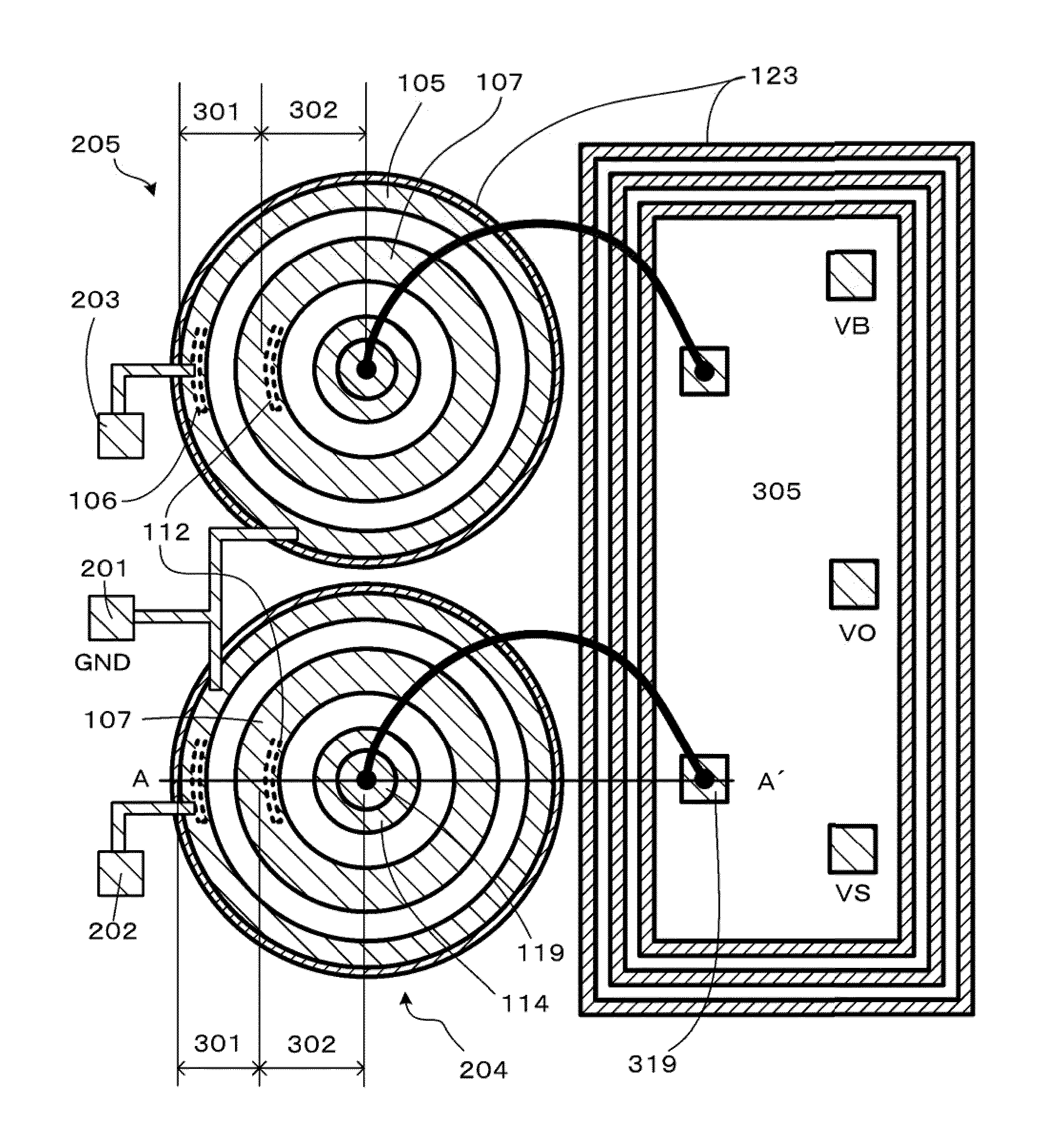
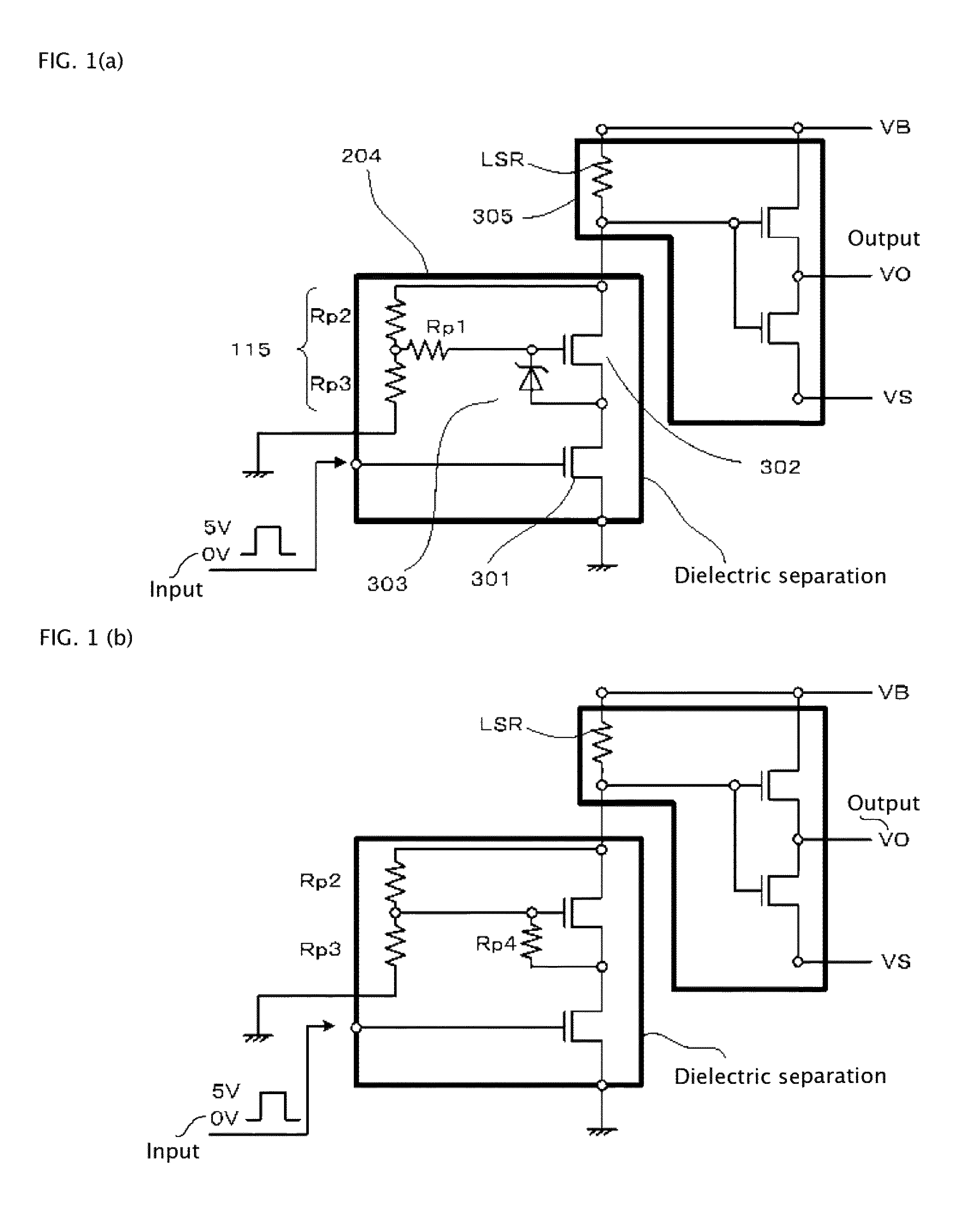
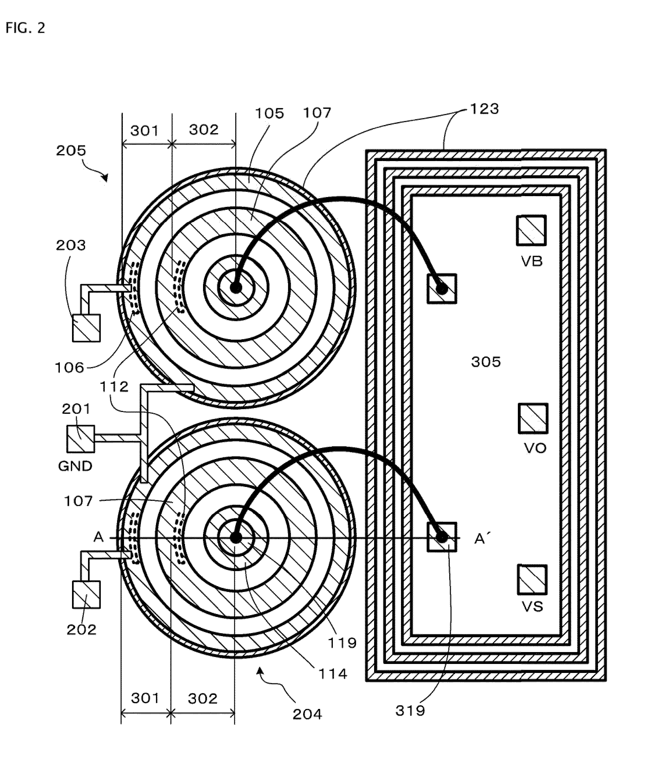
[0070]FIGS. 1(a) and 1(b) show an equivalent circuit diagram of an HVIC including a high-voltage semiconductor device according to the present invention. The constructions of FIGS. 1(a) and 1(b) are different in that a Zener diode 303 is used between a gate and a source of the second stage transistor 302 in the construction of FIG. 1(a) whereas a resistance element Rp4 is employed at that place in the construction of FIG. 1(b). FIG. 2 is a schematic plan view of the high-voltage semiconductor device 204 shown in FIGS. 1(a) and 1(b), another high-voltage semiconductor device 205 (not shown in FIGS. 1(a) and 1(b)), and a floating reference gate drive circuit region 305.

[0071]FIGS. 1(a) and 1(b) show block circuit diagrams in simplified representation for a level sifter input to the HVIC, a level shift resistance LSR, and a high side driving circuit in the floating reference gate drive circuit region 305. A set signal is inputted to the first stage transistor 301 of the high-voltage se...

second embodiment

[0089]FIG. 10 is a sectional view of an essential part of another embodiment example of a high-voltage semiconductor device of the invention.

[0090]This second embodiment differs from the first embodiment in that an NMOSFET 304 is added between the first stage transistor 301 and the second stage transistor 302 to construct a three stage construction with three NMOSFETs connected in series.

[0091]The NMOSFET 304 is formed, similar to the second stage transistor 302, in a ring shaped planar configuration of a p type well diffusion layer 1111 reaching the embedded dielectric layer 200. The p type well diffusion layer 1111 isolates the NMOSFET 304 from the first stage transistor 301. In the surface region of the p type well diffusion layer 1111, a source n+ layer 1091 and a well pick up p+ layer 1101 are formed. A source electrode 1074 connected to the source n+ layer 1091 and the well pick up p+ layer 1101 is connected to the drain electrode 1072 of the first stage transistor 301. A drai...


PUM


Abstract

Aspects of the present invention provide a high-voltage semiconductor device and a high voltage integrated circuit device while minimizing or eliminating the need for the addition of back surface steps. Aspects of the invention provide a high-voltage semiconductor device that achieves, low voltage driving and quick response by way of stable high voltage wiring and a low ON voltage. In some aspects of the invention, a high-voltage semiconductor device can include a semiconductor layer is formed on a support substrate interposing an embedded oxide film therebetween. A high potential side second stage transistor and a low potential side first stage transistor surrounding the second stage transistor are formed on the surface region of the semiconductor layer. The source electrode of the second stage transistor is connected to the drain electrode of the first stage transistor. A drain electrode of the second stage transistor is connected to a drain pad.

Description

CROSS-REFERENCE TO RELATED APPLICATION[0001]This application claims the benefit under 35 U.S.C. §119(a)-(d) of Japanese Patent Application No. 2009-139123, filed on Jun. 10, 2009, currently pending, the contents of which are incorporated herein by reference.BACKGROUND[0002]1. Field of the Invention[0003]The present invention relates to high-voltage semiconductor devices using an SOI (silicon on insulator) substrate, the devices being mainly intended for use in a power conversion integrated circuit represented by an HVIC (high voltage integrated circuit). The devices can be used for an LDMOSFET (lateral double diffused MOSFET) of a high withstand voltage class in the range of 100 V to 1,200 V.[0004]2. Description of the Related Art[0005]Recently, with a demand for high withstand voltage of a power IC containing a high withstand voltage element, SOI substrates are attracting attention, which allow complete isolation between elements by trench dielectric isolation and dielectric insula...

Claims


Application Information

Patent Timeline
Patent Type & Authority Patents(United States)
IPC IPC(8): H01L27/06
CPCH01L24/05H01L24/06H01L24/48H01L27/0207H01L27/088H01L27/1203H01L29/7817H01L2924/1306H01L2224/05552H01L2224/02166H01L2924/00014H01L2924/01033H01L2924/01023H01L2924/01019H01L29/0696H01L29/1095H01L29/402H01L29/405H01L29/42368H01L29/4238H01L29/7821H01L29/7824H01L2224/04042H01L2224/05599H01L2224/45124H01L2224/48091H01L2224/4813H01L2224/48464H01L2224/48699H01L2924/01004H01L2924/01005H01L2924/01007H01L2924/01013H01L2924/01014H01L2924/01015H01L2924/01031H01L2924/01082H01L2924/05042H01L2924/13055H01L2924/13091H01L2924/14H01L2924/19041H01L2924/19042H01L2924/19043H01L2924/30105H01L2924/01006H01L2924/00H01L2924/12035H01L2924/12036H01L24/45H01L2224/05555H01L21/76224
Inventor YAMAJI, MASAHARU
Owner FUJI ELECTRIC CO LTD
Why Eureka
Try Eureka