Semiconductor device

a technology of semiconductor devices and semiconductors, applied in semiconductor devices, digital storage, instruments, etc., can solve the problems of short data retention period, difficult loss of memory content, so as to reduce power consumption sufficiently, reduce the frequency of refresh operation, and reduce the current of the state

Active Publication Date: 2012-10-16
SEMICON ENERGY LAB CO LTD
View PDF144 Cites 46 Cited by
  • Summary
  • Abstract
  • Description
  • Claims
  • Application Information

AI Technical Summary

Benefits of technology

[0030]A transistor using an oxide semiconductor has extremely low off-state current; therefore, by using the transistor, stored contents can be retained for extremely a long time. That is, refresh operation can become unnecessary or frequency of refresh operation can be reduced considerably, so that power consumption can be reduced sufficiently. Further, even in the case where power is not supplied, stored contents can be retained for a long time.
[0031]In addition, high voltage is not needed for writing data and there is no problem of deterioration of elements. Further, writing of data is performed depending on an on state and an off state of the transistor, so that high-speed operation can be easily realized. Additionally, there is an advantage that operation for erasing former data is not needed when rewriting of data is performed.
[0032]Further, the transistor using a material other than an oxide semiconductor can operate at sufficiently high speed, whereby stored contents can be read out at high speed.

Problems solved by technology

In addition, there is leakage current in a transistor included in a memory element and charge stored in the capacitor flows or a charge flows into the capacitor even if the transistor is not selected, whereby data retention period is short.
Therefore, it is necessary to perform writing again in a predetermined cycle (refresh operation) and it is difficult to reduce power consumption sufficiently.
Further, since memory content is lost when the power is not supplied to a DRAM, another memory device using a magnetic material or an optical material is needed to stored memory for a long period.
However, there is a problem in that a cost per storage capacity becomes high because a circuit such as a flip flop is used.
Further, in view of the point that stored contents are lost when the power is not supplied, an SRAM is not superior to a DRAM.
However, in a flash memory, there is a problem in that a memory element does not function after performing writing a predetermined number of times because a gate insulating layer included in the memory element is deteriorated due to tunnel current which occurs when performing writing.
However, a complicated peripheral circuit is needed to realize the method.
Even if such a method is employed, the basic problem of lifetime is not resolved.
That is, a flash memory is unsuitable for application in which data is written with high frequency.
Further, high voltage is required to retain charge in the floating gate or to remove the charge in the floating gate.
Furthermore, a relatively long time is required for retaining or removing a charge and the speed of writing and erasing cannot easily be increased.

Method used


Image

  • Semiconductor device
  • Semiconductor device
  • Semiconductor device

Examples


embodiment 1

[0072]In this embodiment, structures and manufacturing methods of semiconductor devices according to one embodiment of the disclosed invention are described with reference to FIG. 1, FIGS. 2A and 2B, FIGS. 3A to 3H, FIGS. 4A to 4G, FIGS. 5A to 5D, FIG. 6, FIGS. 7A and 7B, FIGS. 8A and 8B, and FIGS. 9A and 9B.

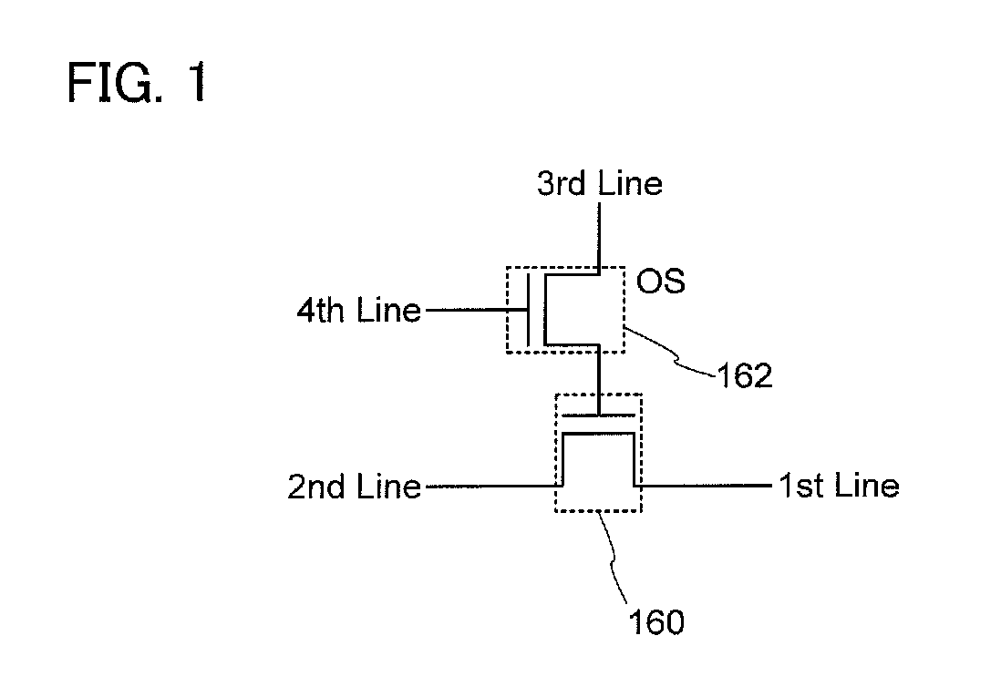
[0073]FIG. 1 illustrates an example of a circuit configuration of a semiconductor device. The semiconductor device includes a transistor 160 formed using a material other than an oxide semiconductor and a transistor 162 formed using an oxide semiconductor. Note that a mark “OS” is added to the transistor 162 in FIG. 1 to show that the transistor 162 is formed using an oxide semiconductor (OS).

[0074]Here, a gate electrode of the transistor 160 is electrically connected to one of a source electrode and a drain electrode of the transistor 162. A first wiring (which is denoted as “1st Line” and also called a source line) and a second wiring (which is denoted as “2nd Line” and also c...

modification example

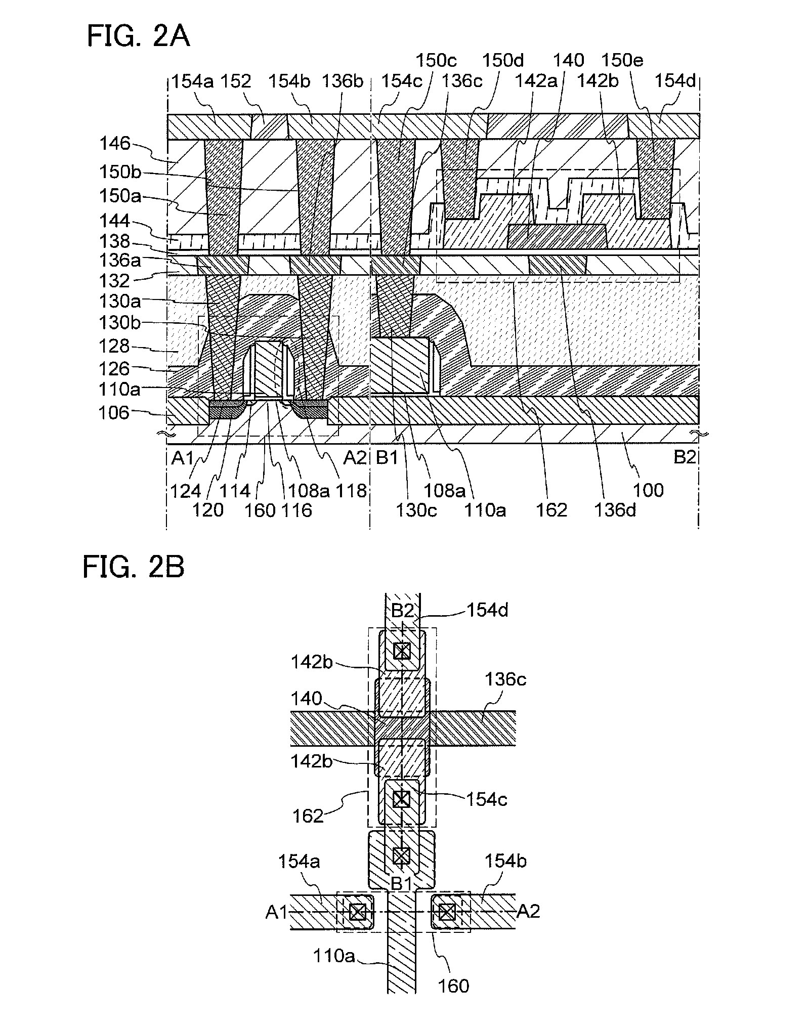
[0194]Modification examples of a structure of a semiconductor device are described with reference to FIG. 6, FIGS. 7A and 7B, FIGS. 8A and 8B, and FIGS. 9A and 9B. Note that in the following modification examples, the structure of the transistor 162 is different from that already described. In other words, the structure of the transistor 160 is similar to that already described.

[0195]In an example illustrated in FIG. 6, the transistor 162 includes the gate electrode 136d under the oxide semiconductor layer 140 and the source or drain electrode 142a and the source or drain electrode 142b which are in contact with the oxide semiconductor layer 140 at a bottom surface of the oxide semiconductor layer 140. Since a plan structure may be appropriately changed corresponding to a cross-sectional structure, only the cross-sectional structure is described here.

[0196]As a large difference between the structure illustrated in FIG. 6 and that illustrated in FIGS. 2A and 2B, there are connection ...

embodiment 2

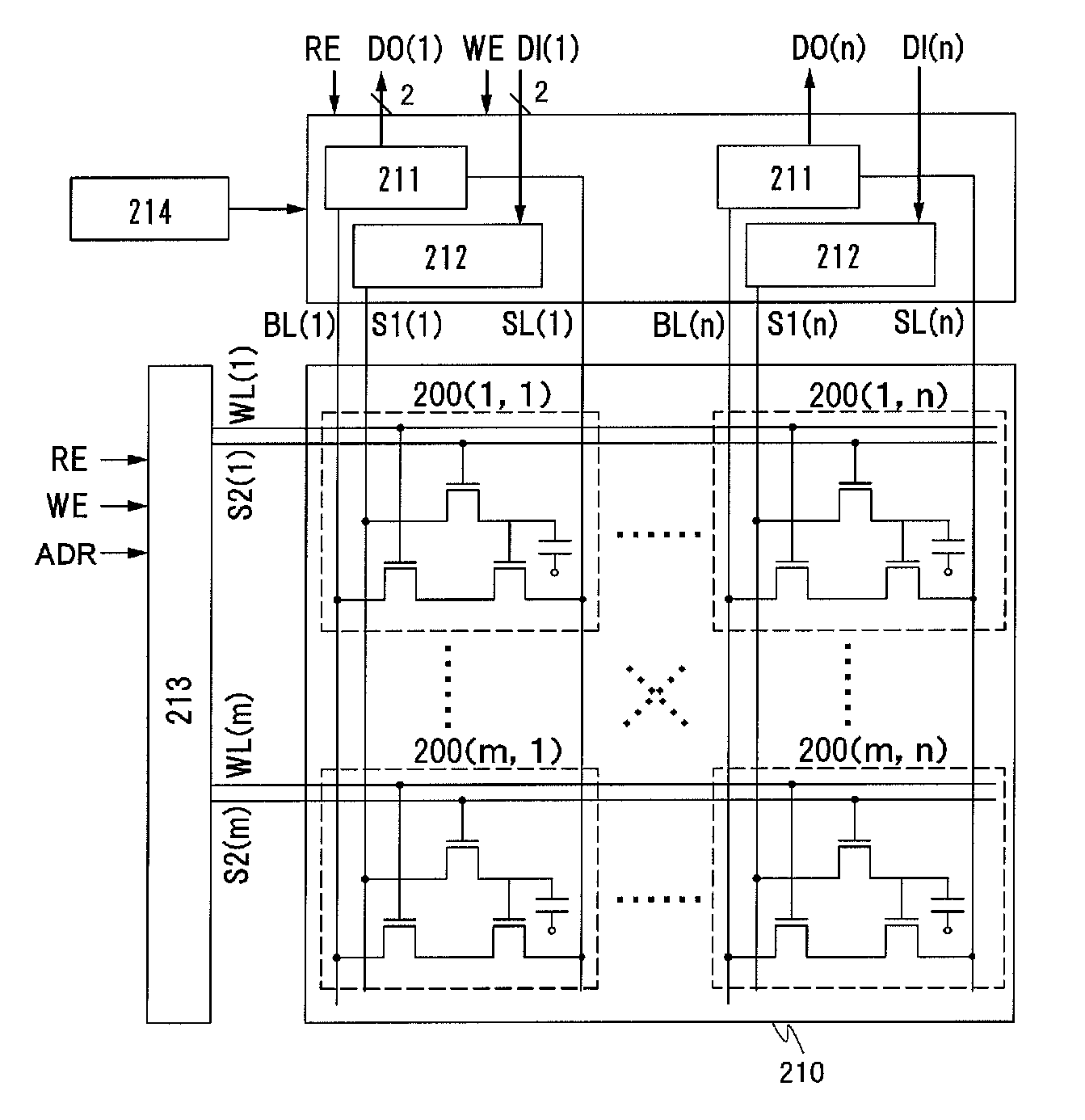
[0222]In this embodiment, a circuit configuration and operation of a semiconductor device according to an embodiment of the present invention are described.

[0223]An example of a circuit diagram of a memory element (hereinafter also referred to as a memory cell) included in the semiconductor device is illustrated in FIG. 10. A memory cell 200 illustrated in FIG. 10 is a multivalued memory cell and includes a source line SL, a bit line BL, a first signal line S1, a second signal line S2, a word line WL, a transistor 201, a transistor 202, a transistor 203, and a capacitor 205. The transistors 201 and 203 are formed using a material other than an oxide semiconductor, and the transistor 202 is formed using an oxide semiconductor.

[0224]Here, a gate electrode of the transistor 201 is electrically connected to one of a source electrode and a drain electrode of the transistor 202. In addition, the source line SL is electrically connected to a source electrode of the transistor 201, and a so...


PUM


Abstract

An object is to provide a semiconductor device having a novel structure. A first wiring; a second wiring; a third wiring, a fourth wiring; a first transistor including a first gate electrode, a first source electrode, and a first drain electrode; a second transistor including a second gate electrode, a second source electrode, and a second drain electrode are included. The first transistor is provided over a substrate including a semiconductor material and a second transistor includes an oxide semiconductor layer.

Description

TECHNICAL FIELD[0001]The present invention relates to a semiconductor device using semiconductor elements and a manufacturing method thereof.BACKGROUND ART[0002]Memory devices using semiconductor elements are roughly classified into volatile memory devices that lose their stored contents when power supply is stopped and non-volatile memory devices that can retain their stored contents even when power supply is stopped.[0003]As a typical example of a volatile memory device, a dynamic random access memory (DRAM) is given. In a DRAM, a transistor included in a memory element is selected and a charge is accumulated in a capacitor, so that data is stored.[0004]Owing to the above-described principle, charge in a capacitor is lost when data is read out in a DRAM; thus, it is necessary to perform writing again so that data is stored again after reading data. In addition, there is leakage current in a transistor included in a memory element and charge stored in the capacitor flows or a charg...

Claims


Application Information

Patent Timeline
Patent Type & Authority Patents(United States)
IPC IPC(8): G11C11/24
CPCG11C11/405H01L27/105G11C11/24H01L27/11551H01L27/1156H01L27/1225G11C7/12G11C2211/4016H01L27/0688H01L27/1108H10B10/125H10B41/70H10B41/20H01L27/0207
Inventor YAMAZAKI, SHUNPEIKOYAMA, JUNKATO, KIYOSHI
Owner SEMICON ENERGY LAB CO LTD
Why Eureka
Try Eureka