Thin film transistor and method of producing the same, display device, image sensor, x-ray sensor, and x-ray digital imaging device

Active Publication Date: 2014-08-21
SAMSUNG DISPLAY CO LTD
View PDF5 Cites 23 Cited by
  • Summary
  • Abstract
  • Description
  • Claims
  • Application Information

AI Technical Summary

Benefits of technology

[0047]According to the invention, there can be provided a thin film transistor which can be produced at 400° C. or less and simultaneously realizes a high field-effect mobility of 20 cm2/Vs or more and a low off-current for

Problems solved by technology

As shown in Table 1, although a thin film transistor in which an active layer is made from polysilicon is capable of having a mobility of approximately 100 cm2/Vs, since the process temperature is 450° C. or more and thus is very high, the thin film transistor can be formed only on a highly heat-resistant substrate and is not suitable for reduction in cost, increase in area, and flexibilizatio

Method used


Image

  • Thin film transistor and method of producing the same, display device, image sensor, x-ray sensor, and x-ray digital imaging device
  • Thin film transistor and method of producing the same, display device, image sensor, x-ray sensor, and x-ray digital imaging device
  • Thin film transistor and method of producing the same, display device, image sensor, x-ray sensor, and x-ray digital imaging device

Examples


examples

[0182]Hereinafter, experimental examples will be described; however, the invention is in no way limited to the examples.

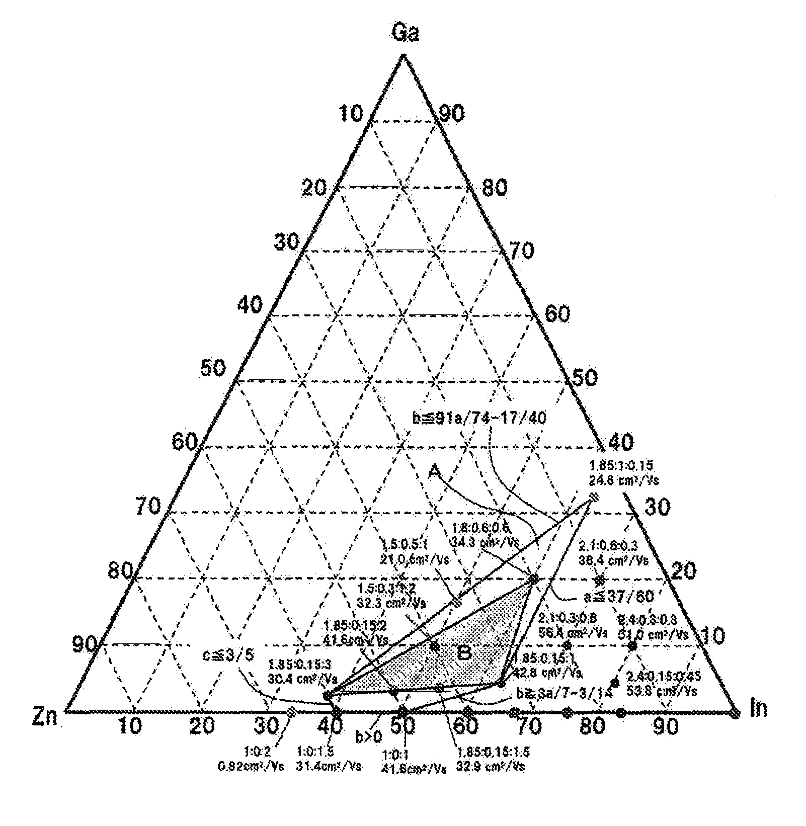
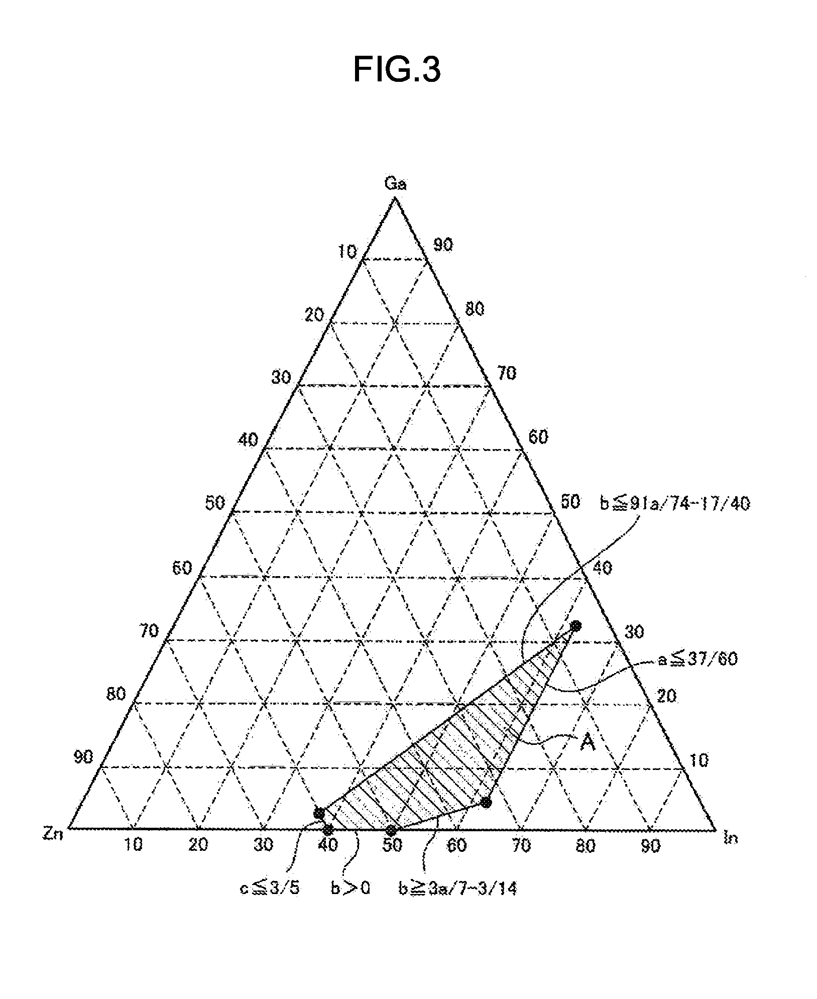
[0183]The present inventors conducted the following experiments and proved that, as the thin film transistor according to the invention, an element having high mobility and a low off-current can be produced in a specific composition range in the first region A1 and the second region A2 forming the oxide semiconductor layer.

[0184]

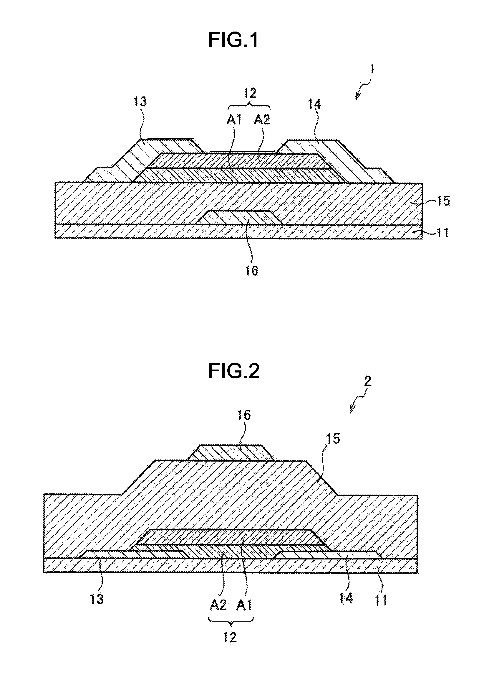
[0185]First, the following bottom gate-top contact type-thin film transistors were produced as Examples 1 to 8 and Comparative Examples 1 to 4.

[0186]As a substrate, a p-type silicon substrate (manufactured by Mitsubishi Materials Corporation) in which an SiO2 oxide film (thickness: 100 nm) was formed on a surface so as to be doped at high concentration was used.

[0187]As an oxide semiconductor layer, a first region was first formed by sputtering such that the thickness of In(a) Ga(b) Zn(c) O(d) in which a>0, b>0, c>0, d>0, and a+b+c=1 was 5 ...


PUM


Abstract

A thin film transistor includes a gate electrode; a gate insulating film which contacts the gate electrode; an oxide semiconductor layer which includes a first region represented by In(a) Ga(b) Zn(c) O(d), wherein 0<a≦37/60, 3a/7−3/14≦b≦91a/74−17/40, b>0, 0<c<3/5, a+b+c=1, and d>0, and a second region represented by In(p) Ga(q) Zn(r) O(s), wherein q/(p+q)>0.250, p>0, q>0, r>0, and s>0, and located farther than the first region with respect to the gate electrode and which is arranged facing the gate electrode with the gate insulating film provided therebetween; and a source electrode and a drain electrode which are arranged so as to be apart from each other and are capable of being electrically conducted through the oxide semiconductor layer.

Description

CROSS-REFERENCE TO RELATED APPLICATIONS[0001]This application is a continuation application of International Application No. PCT / JP2012 / 067508, filed Jul. 9, 2012, the disclosure of which is incorporated herein by reference in its entirety. Further, this application claims priority from Japanese Patent Application No. 2011-177235, filed Aug. 12, 2011, the disclosure of which is incorporated herein by reference in its entirety.TECHNICAL FIELD[0002]The present invention relates to a thin film transistor and a method of producing the same, a display device, an image sensor, an X-ray sensor, and an X-ray digital imaging device.BACKGROUND ART[0003]Recently, a thin film transistor using an In—Ga—Zn—O-based (hereinafter referred to as IGZO) oxide semiconductor thin film in an active layer (channel layer) has been actively researched and developed. The oxide semiconductor thin film can be formed at a low temperature, exhibits higher mobility than that of amorphous silicon, and is transparen...

Claims


Application Information

Patent Timeline
IPC IPC(8): H01L29/786H01L29/66
CPCH01L29/66969H01L29/78693H01L27/14658H01L29/7869H05B33/10H05B33/26H01L21/02422H01L21/02631H01L21/02554H01L21/02565H10K59/1213H01L21/02472H01L21/02483H01L27/14659H10K59/65H01L27/146H01L29/786
Inventor ONO, MASASHITAKATA, MASAHIROTANAKA, ATSUSHISUZUKI, MASAYUKI
Owner SAMSUNG DISPLAY CO LTD
Why Eureka
Try Eureka