

Transmission line, optical module using the same and manufacturing method of optical module
- Summary
- Abstract
- Description
- Claims
- Application Information
AI Technical Summary
Benefits of technology
Problems solved by technology
Method used
Image

Examples
first embodiment
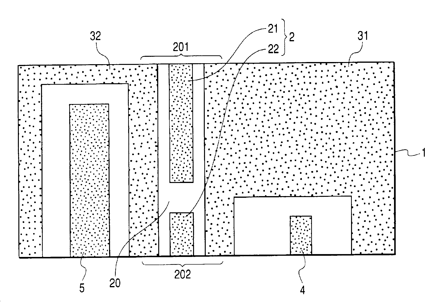
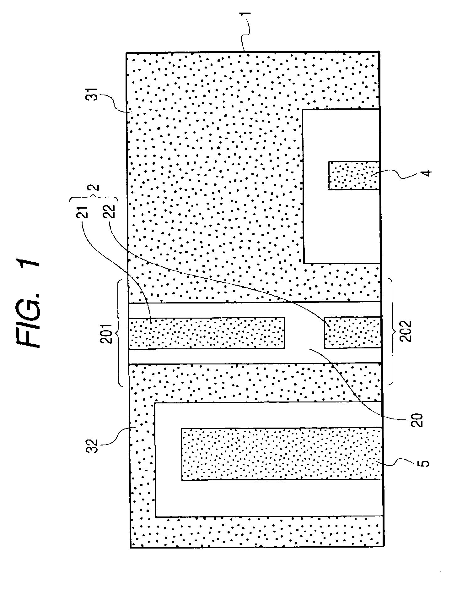
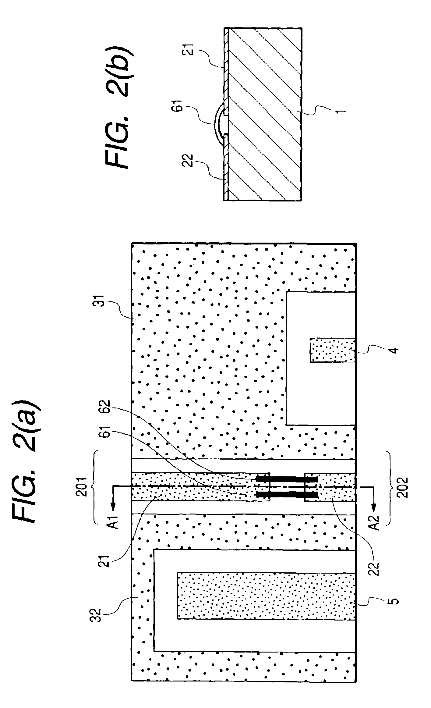
FIG. 1 is a top view showing a first example of a wiring pattern of a transmission line according to the present invention. FIG. 2 is a construction diagram of a transmission line according to the present invention, with the wiring pattern of FIG. 1 being connected for an optical module of 10 Gbit / s, in which FIG. 2(a) is a top view and FIG. 2(b) is a sectional view taken on line A1-A2 of FIG. 2(a). FIG. 3 is a construction diagram with the wiring pattern of FIG. 1 connected for an optical module of 2.5 Gbit / s, in which FIG. 3(a) is a top view and FIG. 3(b) is a sectional view taken on line B1-B2 of FIG. 3(a).
As shown in FIG. 1, a wiring conductor of the illustrated transmission line is formed on a surface of a substrate 1 which is formed by a dielectric. The transmission line is in the form of a coplanar line in which first and second ground wiring conductors 31, 32 are formed on both sides of a signal wiring conductor 2. The signal wiring conductor 2 is electrically insulated in a...
second embodiment
the present invention will be described below with reference to FIGS. 11 to 13.
FIG. 11 is a top view showing a wiring pattern of a transmission line according to a second embodiment of the present invention. FIG. 12 is a construction diagram showing the transmission line of the second embodiment with the wiring pattern of FIG. 11 being connected for an optical module of 10 Gbit / s. FIG. 13 is a construction diagram of the transmission line of the second embodiment with the wiring pattern of FIG. 11 being connected for an optical module of 2.5 Gbit / s.
Although in the embodiment of FIG. 3 there are used one first electrode serving as an inductor and one second electrode as a capacitor, plural such inductors and capacitors may be present. In the embodiment illustrated in FIG. 13 there are used two inductors and three capacitors.
In FIG. 11, which illustrates a wiring pattern according to a second embodiment of the present invention, a signal wiring conductor is composed of a first signal ...
PUM
 Abstract
Description
Claims
Application Information