Semiconductor device and method for driving semiconductor device

a semiconductor device and semiconductor technology, applied in the field of semiconductor devices, can solve the problems of limited reduction of the operation voltage of the memory cell, fluctuation of the potential needed for driving a plurality of memory cells, and operation errors, so as to achieve the effect of reducing the frequency of refresh operation, storing data for an extremely long time, and reducing power consumption

Inactive Publication Date: 2013-09-24
SEMICON ENERGY LAB CO LTD
View PDF138 Cites 27 Cited by
  • Summary
  • Abstract
  • Description
  • Claims
  • Application Information

AI Technical Summary

Benefits of technology

[0014]In view of the foregoing problems, an object of one embodiment of the disclosed invention is to provide a semiconductor device with a novel structure in which stored data can be held even when power is not supplied and there is no limit on the number of times of writing, and to provide a method for driving the semiconductor device. It is another object to provide a semiconductor device in which, by reducing variation (distribution width) in the threshold voltages of memory cells after writing, the operation voltage can be reduced, the storage capacity can be increased, or operation such as writing, holding, or reading can be surely performed, and to provide a method for driving the semiconductor device.
[0015]In one embodiment of the disclosed invention, a semiconductor device is manufactured using an oxide semiconductor. In particular, a highly purified oxide semiconductor is used. A transistor formed using an, oxide semiconductor can hold data for a long time because leakage current thereof is extremely low. In the case of using a highly purified oxide semiconductor, leakage current is much lower and thus data can be held for an extremely long time.
[0036]Since the off-current of a transistor including an oxide semiconductor is extremely low, stored data can be held for an extremely long time by using the transistor, even if power is not supplied. In other words, power consumption can be sufficiently reduced because refresh operation becomes unnecessary or the frequency of refresh operation can be extremely low.
[0037]In a semiconductor device according to the disclosed invention, even when the threshold voltage of a transistor included in a memory cell fluctuates, variation (distribution width) in the threshold voltages of a plurality of memory cells after writing can be reduced, whereby the operation voltage of the semiconductor device can be reduced. A memory can be multi-valued without increasing the operation voltage and the area of a memory cell, so that the storage capacity per unit area of the semiconductor device can be increased. A semiconductor device in which operation such as writing, holding, or reading can be surely performed can be provided.
[0038]Further, the semiconductor device according to the disclosed invention does not need high voltage for data writing and there is no problem of element deterioration. For example, unlike a conventional nonvolatile memory, it is not necessary to inject and extract electrons or holes into and from a floating gate, and thus a problem such as deterioration of a gate insulating layer does not occur at all. In other words, the semiconductor device according to the disclosed invention does not have a limit on the number of times of rewriting which is a problem in a conventional nonvolatile memory, and reliability thereof is drastically improved. Furthermore, data is written by turning on or off the transistor, whereby high-speed operation can be easily realized. In addition, there is an advantage in that operation for erasing data is not needed.
[0039]Since a transistor including a material other than an oxide semiconductor can operate at sufficiently high speed, a semiconductor device in which the transistor is used in combination with a transistor including an oxide semiconductor can perform operation (e.g., data reading) at sufficiently high speed. Further, a transistor including a material other than an oxide semiconductor can favorably realize a variety of circuits (such as a logic circuit or a driver circuit) which is required to operate at high speed.

Problems solved by technology

In addition to the above problems, fluctuation in the threshold voltage of a transistor included in a memory cell may cause fluctuation in potentials needed for driving a plurality of memory cells (such a potential is also referred to as the threshold voltage of a memory cell).
If the operation voltages of the memory cells are determined without consideration of the fluctuation in the threshold voltages of the memory cells, an operation error might be caused.
This has limited a reduction in the operation voltages of the memory cells.
Moreover, in the case where a memory cell is multi-valued, the operation voltage is increased; therefore, it has been difficult to increase the storage capacity without increasing the operation voltage and the area of the memory cell.
A transistor formed using an, oxide semiconductor can hold data for a long time because leakage current thereof is extremely low.
In the case of using a highly purified oxide semiconductor, leakage current is much lower and thus data can be held for an extremely long time.

Method used


Image

  • Semiconductor device and method for driving semiconductor device
  • Semiconductor device and method for driving semiconductor device
  • Semiconductor device and method for driving semiconductor device

Examples


embodiment 1

(Embodiment 1)

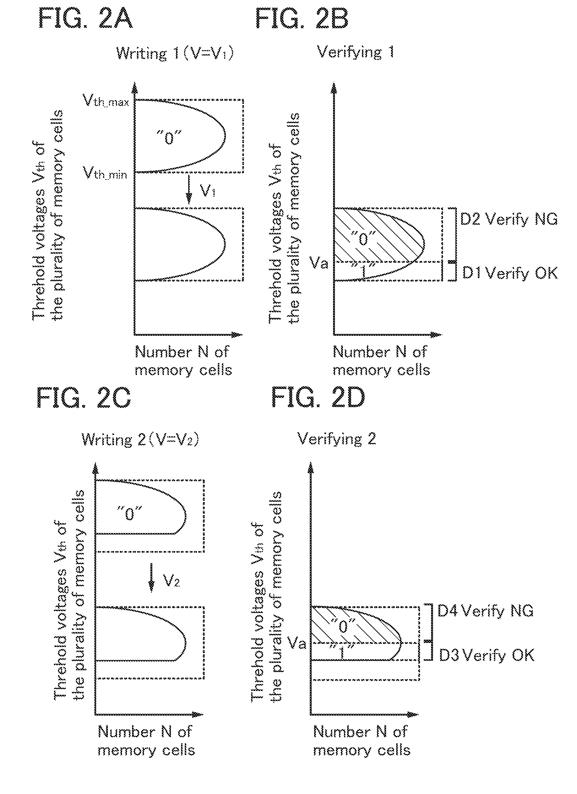
[0091]In this embodiment, a structure and operation of a semiconductor device according to one embodiment of the disclosed invention will be described with reference to FIG. 1, FIGS. 2A to 2D, FIGS. 3A to 3D, and FIGS. 4A and 4B.

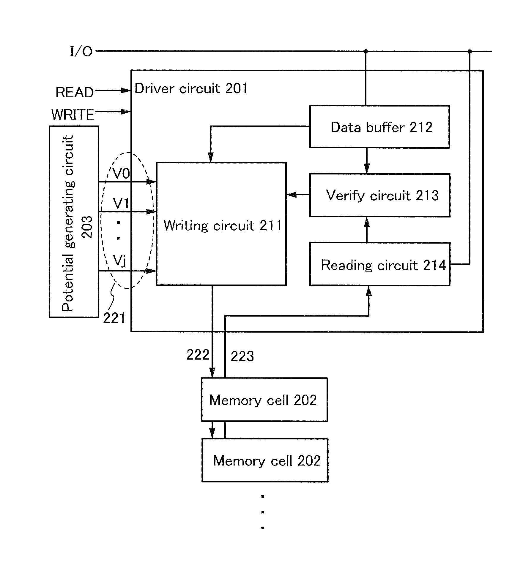
[0092]FIG. 1 is an example of a block diagram of a semiconductor device including memory cells.

[0093]The semiconductor device includes a plurality of memory cells 202, a driver circuit 201, and a potential generating circuit 203. The driver circuit 201 includes a data buffer 212, a writing circuit 211, a reading circuit 214, and a verifying circuit 213. Each of the plurality of memory cells 202 includes a transistor (not shown) including an oxide semiconductor and a transistor (not shown) including a material other than an oxide semiconductor. Further, the semiconductor device includes a wiring for supplying an input / output signal (I / O) (also referred to as a data input / output line), a wiring for supplying a read signal (READ), and a wiring for...

embodiment 2

(Embodiment 2)

[0146]In this embodiment, a circuit configuration and operation of a memory cell included in a semiconductor device according to one embodiment of the disclosed invention will be described with reference to FIGS. 5A1, 5A2, and 5B. Note that in some circuit diagrams, “OS” is written beside a transistor in order to indicate that the transistor includes an oxide semiconductor.

[0147]In a memory cell illustrated in FIG. 5A-1, a first wiring (a 1st Line) and a source electrode (or a drain electrode) of a transistor 160 are electrically connected to each other, and a second wiring (a 2nd Line) and the drain electrode (or the source electrode) of the transistor 160 are electrically connected to each other. In addition, a third wiring (a 3rd Line) and a source electrode (or a drain electrode) of a transistor 162 are electrically connected to each other, and a fourth wiring (a 4th Line) and a gate electrode of the transistor 162 are electrically connected to each other. Further,...

embodiment 3

(Embodiment 3)

[0182]In this embodiment, application examples of a semiconductor device according to one embodiment of the disclosed invention will be described with reference to FIGS. 6A to 6C. Here, examples of a memory device will be described. Note that in some circuit diagrams, “OS” is written beside a transistor in order to indicate that the transistor includes an oxide semiconductor.

[0183]FIGS. 6A to 6C are each a circuit diagram of a semiconductor device, which can be used as a memory device, including a plurality of semiconductor devices (hereinafter also referred to as memory cells) illustrated in FIG. 5A1. FIGS. 6A and 6B are circuit diagrams of so-called NAND semiconductor devices in which memory cells are connected in series, and FIG. 6C is a circuit diagram of a so-called NOR semiconductor device in which memory cells are connected in parallel.

[0184]The semiconductor device in FIG. 6A includes a source line SL, a bit line BL, a first signal line S1, m second signal line...


PUM


Abstract

A semiconductor device with a novel structure is provided, in which the operation voltage is reduced or the storage capacity is increased by reducing variation in the threshold voltages of memory cells after writing. The semiconductor device includes a plurality of memory cells each including a transistor including an oxide semiconductor and a transistor including a material other than an oxide semiconductor, a driver circuit that drives the plurality of memory cells, and a potential generating circuit that generates a plurality of potentials supplied to the driver circuit. The driver circuit includes a data buffer, a writing circuit that writes one potential of the plurality of potentials into each of the plurality of memory cells as data, a reading circuit that reads the data written into the memory cells, and a verifying circuit that verifies whether the read data agrees with data held in the data buffer or not.

Description

BACKGROUND OF THE INVENTION[0001]1. Field of the Invention[0002]The invention disclosed herein relates to a semiconductor device using a semiconductor element and a method for driving the semiconductor device.[0003]2. Description of the Related Art[0004]Memory devices using semiconductor elements are broadly classified into two categories: a volatile device that loses stored data when power supply stops, and a nonvolatile device that holds stored data even when power is not supplied.[0005]A typical example of a volatile memory device is a dynamic random access memory (DRAM). A DRAM stores data in such a manner that a transistor included in a memory element is selected and charge is stored in a capacitor.[0006]When data is read from a DRAM, charge in a capacitor is lost according to the above principle; thus, another writing operation is necessary every time data is read. Moreover, a transistor included in a memory element has leakage current (off-state current) between a source and ...

Claims


Application Information

Patent Timeline
Patent Type & Authority Patents(United States)
IPC IPC(8): G11C11/34
CPCG11C11/405G11C11/4076G11C11/5685G11C13/0007G11C13/003G11C13/0033G11C13/0064G11C13/0069G11C2213/79G11C2211/4016G11C5/147G11C7/00G11C11/4074G11C5/063G11C11/40
Inventor SEKINE, YUSUKEKATO, KIYOSHI
Owner SEMICON ENERGY LAB CO LTD
Why Eureka
Try Eureka