
Electronic component mounted structure

a technology for mounting structures and electronic components, applied in the field of mounting electronic components, can solve the problems of reducing the bonding strength at the portion, increasing the electrical resistance, and reducing so as to improve the reliability of the connection and avoid electromigration

Active Publication Date: 2012-11-06
SHINKO ELECTRIC IND CO LTD
View PDF17 Cites 5 Cited by
  • Summary
  • Abstract
  • Description
  • Claims
  • Application Information

AI Technical Summary

Benefits of technology

[0013]An object of the present invention is to provide an electronic component mounted structure which substantially eliminates problems such as an increase in the electrical resistance, an open circuit or the like, due to electromigration at the connection portion at the time of use (at the time of conducting a current) after an electronic component is mounted on a wiring board, and which consequently contributes to an improvement in the reliability of connection.
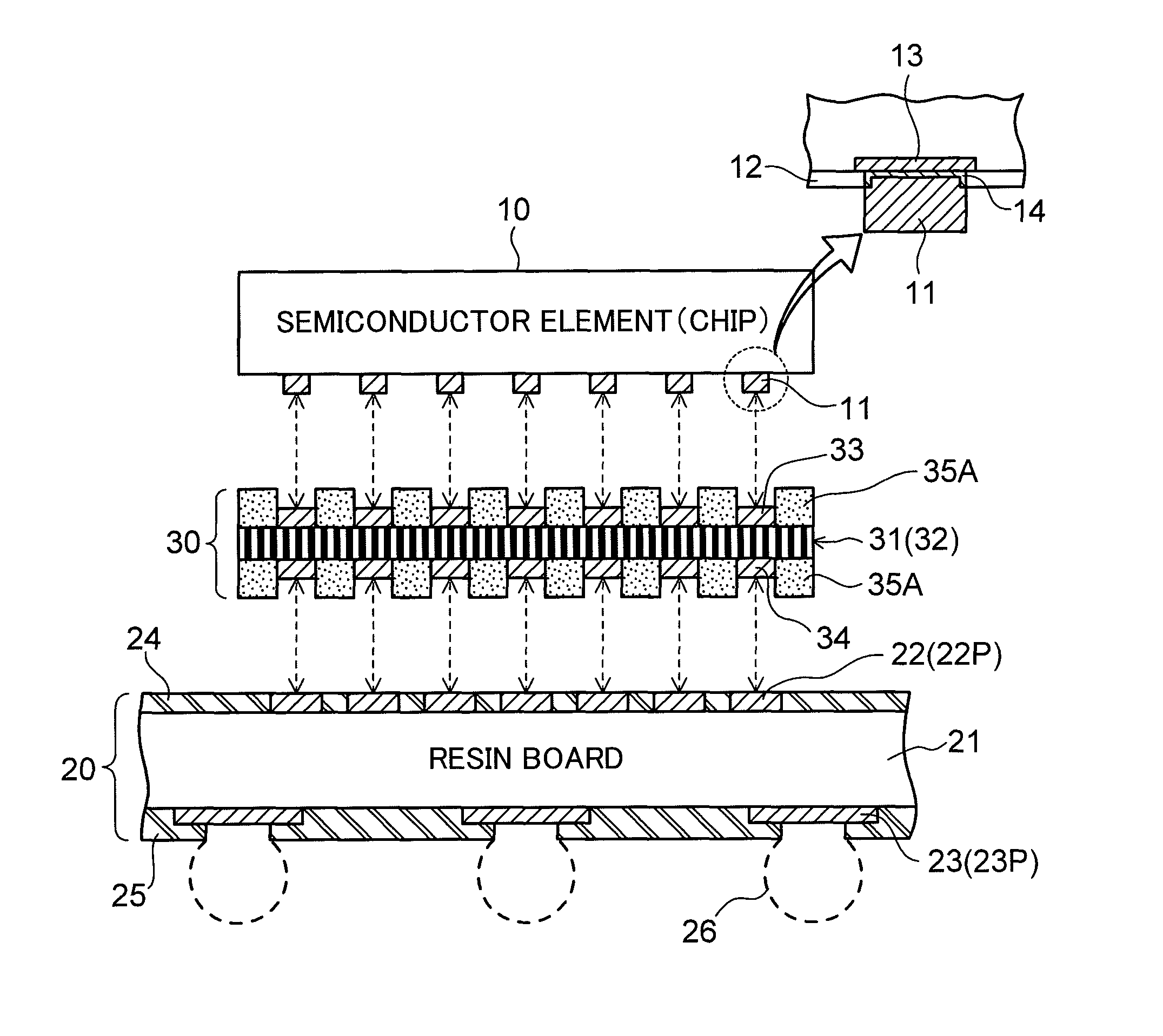
[0015]In a conventional structure, a chip (electronic component) and a package (wiring board) are connected to each other with a solder bump interposed between a terminal of the chip and a corresponding terminal (pad) on the package. In contrast, in the electronic component mounted structure according to the present invention, the electronic component and the wiring board are connected to each other with the plurality of filamentous conductors interposed between the terminal of the electronic component and the corresponding terminal on the wiring board. Namely, the electronic component is mounted on the wiring board without solder which is one of low-melting-point metals and which readily causes electromigration.
[0016]According to this structure, it is possible to substantially eliminates problems such as encountered in the prior art (an increase in the electrical resistance, an open circuit or the like, due to electromigration at the connection portion between the chip and the board) at the time of use after the mounting (at the time of conducting a current). This contributes to an improvement in the reliability of connection between the electronic component and the wiring board.

Problems solved by technology

This causes the following problems at the time of use (at the time of conducting a current) after the chip is mounted on the package.
As a result, a void is produced in a portion of the connection portion, which increases the electrical resistance and reduces the bonding strength at the portion.
The phenomenon accumulatively causes problems such as an increase in the electrical resistance, an open circuit or the like at the connection portion, and thus lowers a reliability in the connection.

Method used


Image

  • Electronic component mounted structure
  • Electronic component mounted structure
  • Electronic component mounted structure

Examples


Embodiment Construction

[0025]Description is given below with regard to preferred embodiments of the present invention with reference to the accompanying drawings.

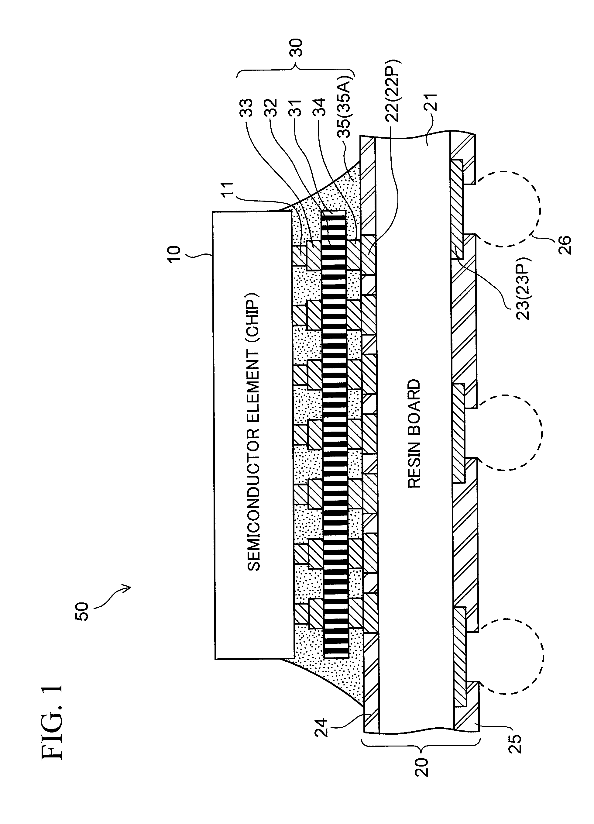
[0026]FIG. 1 shows a sectional view of an electronic component mounted structure according to an embodiment of the present invention.

[0027]The electronic component mounted structure 50 according to the present embodiment basically includes a semiconductor element (chip) 10 as an electronic component to be mounted, a wiring board (package) 20 for mounting the semiconductor element (chip) 10, and a board 30 interposed between the chip 10 and the package 20 and serving as an interposer for electrically connecting and mechanically bonding the two. Namely, the electronic component mounted structure 50 of this embodiment constitutes a semiconductor device. The board 30 interposed between the chip 10 and the package 20 is a member characterizing the invention, and is referred to as a “board for interposer” for the convenience of distinguishing the board...


PUM


Abstract

An electronic component (chip) mounted structure includes a chip having a terminal, a wiring board having a terminal electrically connected to the terminal of the chip, and an interposing board disposed between the chip and the wiring board and having a structure including an insulating base material provided with a large number of filamentous conductors penetrating the insulating base material in a thickness direction thereof. The terminal of the chip is electrically connected to the terminal of the wiring board via a plurality of filamentous conductors provided in the interposing board.

Description

CROSS-REFERENCE TO RELATED APPLICATIONS[0001]This application is based on and claims priority of Japanese Patent Application No. 2009-120634 filed on May 19, 2009, the entire contents of which are incorporated herein by reference.BACKGROUND OF THE INVENTION[0002](a) Field of the Invention[0003]The present invention relates to a technology for mounting an electronic component such as a semiconductor element or the like on a wiring board. More particularly, it relates to an electronic component mounted structure in which a board serving as an interposer is interposed between a wiring board and an electronic component mounted thereon.[0004]In such a mounted structure, the wiring board plays a role in mounting of an electronic component such as a semiconductor element or the like, and thus is also referred to as a “semiconductor package” or simply a “package” for convenience in the description below.[0005](b) Description of the Related Art[0006]Flip chip bonding is one of methods for mo...

Claims


Application Information

Patent Timeline
Patent Type & Authority Patents(United States)
IPC IPC(8): H05K1/11
CPCH01L24/29H01L24/32H05K3/325H01L23/49827H01L23/49816H01L2224/29386H01L23/49833H01L24/13H01L24/16H01L24/83H01L2224/13147H01L2224/16225H01L2224/83192H01L2224/83194H01L2924/01013H01L2924/01029H01L2924/0103H01L2924/01046H01L2924/01047H01L2924/0105H01L2924/01059H01L2924/01078H01L2924/01079H01L2924/01082H01L2924/01322H01L2924/09701H01L2924/14H01L2924/15311H01L2924/30105H01L2924/3025H05K3/305H05K2201/09945H05K2201/10378H05K2201/10674H05K2201/10977H01L2224/29H01L2224/2919H01L2924/01005H01L2924/01006H01L2924/01024H01L2924/01033H01L2924/014H01L2924/0665H01L2224/29101H01L2924/0132H01L2224/32225H01L2224/73204H01L2924/0133H01L2924/15724H01L2224/29111H01L2924/00013H01L2224/2929H01L2924/00H01L2924/00015H01L2924/3512H01L2924/00014H01L2924/05432H01L2924/05042H01L2924/05032H01L2924/05442H01L2224/29099H01L2224/29199H01L2224/29299H01L2224/05001H01L2224/05022H01L2224/05124H01L2224/05166H01L2224/05171H01L2224/05572H01L2224/05647H01L2224/16237H01L2224/81191H01L2924/15788H01L2924/351
Inventor KOBAYASHI, TSUYOSHIHORIUCHI, MICHIOSHIMIZU, YUKIOTOKUTAKE, YASUE
Owner SHINKO ELECTRIC IND CO LTD
Learn More