Wiring structure, display apparatus, and semiconductor device

a display device and wiring technology, applied in the direction of semiconductor devices, semiconductor/solid-state device details, electrical apparatus, etc., can solve the problems of increased production cost, reduced productivity, signal delay and power loss attributable to high wiring resistance, etc., to achieve excellent contact resistance, increase process margins, and high productivity

Active Publication Date: 2013-01-31
KOBE STEEL LTD
View PDF0 Cites 7 Cited by
  • Summary
  • Abstract
  • Description
  • Claims
  • Application Information

AI Technical Summary

Benefits of technology

[0022]The present invention can provide a direct contact technology that enables a Cu alloy layer and a semiconductor layer to come into direct contact with each other, offers excellent contact resistance between the Cu alloy layer and the semiconductor layer, and achieves high productivity and further enlarged process margins. In particular, a technology that is less susceptible to variations in various processing conditions (variation in system performance, instability, unexpected contamination, contamination that is hard to control, etc.), that does not need stringent condition control, and that has less limitations on process conditions can be provided. Since the first layer of the Cu alloy layer is a Cu—X alloy layer (first layer) containing X as an alloy component (X is at least one selected from the group consisting of Zn, Ni, Ti, Al, Mg, Ca, W, Nb, and Mn) and the second layer is a layer composed of Cu or a Cu alloy mainly composed of Cu and having an electrical resistivity lower than that of the first layer, the adhesion to the semiconductor layer is improved, low contact resistance is achieved, and the increase in electrical resistance of the Cu alloy layer as a whole can be suppressed.

Problems solved by technology

However, as the size of the display devices increases and the image quality improves, a problem of signal delay and power loss attributable to high wiring resistance has become noticeable.
Second, when Cu in the Cu-based alloy wiring film diffuses into the semiconductor as described above and a reaction layer between the semiconductor layer and Cu is formed, the Cu-based alloy wiring film becomes detached from the semiconductor layer at this reaction layer, which is a problem.
In particular, a film-forming system equipped with an extra film-forming chamber for forming barrier metal layers (typically, a cluster tool in which a plurality of film-forming chambers are connected to transfer chambers) must be used, and this increases the production cost and decreases the productivity.

Method used


Image

  • Wiring structure, display apparatus, and semiconductor device
  • Wiring structure, display apparatus, and semiconductor device
  • Wiring structure, display apparatus, and semiconductor device

Examples


first embodiment

of the Present Invention

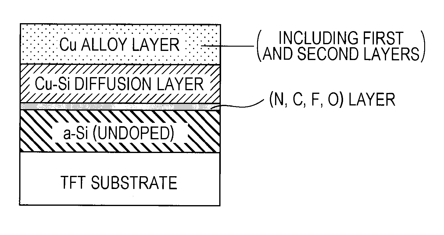
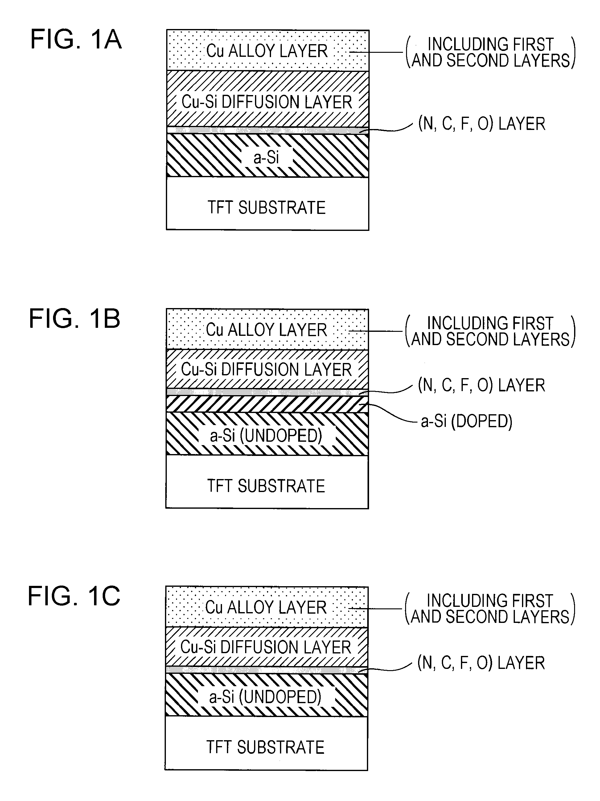
[0045]A first embodiment of the TFT according to the present invention is shown in FIG. 1A. A structure shown in FIG. 1A includes a first semiconductor layer on a TFT substrate; a two-layer structure directly on the first semiconductor layer, the two-layer structure including a (N, C, F, O) layer and a Cu—Si diffusion layer; and a Cu alloy layer (including a first layer and a second layer) directly on the two-layer structure. The structure shown in FIG. 1A is obtained by forming a (N, C, F, O) layer, then forming a second semiconductor layer and a Cu alloy layer (multilayer structure), and then applying a heat history at about 150° C. or higher.

[0046]In the first embodiment, the (N, C, F, O) layer contains at least one element selected from the group consisting of nitrogen, carbon, fluorine, and oxygen. Since the (N, C, F, O) layer is formed so as to substantially cover the entire surface of the semiconductor layer, the (N, C, F, O) layer effectively serves a...

second embodiment

of the Present Invention

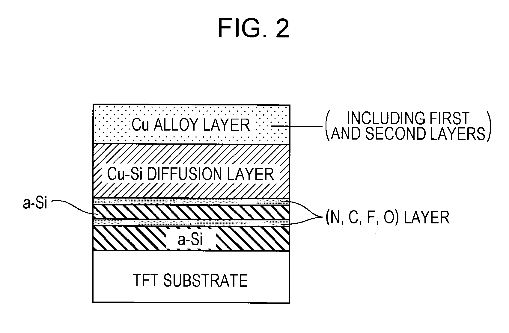
[0083]A second embodiment of the TFT according to the present invention is an example that has a first semiconductor layer, a (N, C, F, O) layer, and another first semiconductor layer between the TFT substrate and the (N, C, F, O) layer constituting the two-layer structure in the first embodiment described above. In particular, as shown in FIG. 2, a first semiconductor layer, a (N, C, F, O) layer, and another first semiconductor layer are stacked in that order on a TFT substrate, a two-layer structure including a (N, C, F, O) layer and a Cu—Si diffusion layer is disposed thereon, and a Cu alloy layer is directly formed on the two-layer structure.

third embodiment

of the Present Invention

[0084]A first embodiment of a MOSFET according to the present invention is shown in FIG. 4. In FIG. 4, a two-layer structure including a (N, C, F, O) layer and a Cu—Si diffusion layer is directly formed on single crystal Si and a Cu alloy layer is directly formed on the two-layer structure. This structure is formed by the steps shown in FIG. 5. That is, among N, C, F, and O, for example, nitrogen is implanted into a single crystal Si substrate by an ion implantation method or the like. During this process, implanted nitrogen exhibits a substantially Gaussian distribution in the depth direction around a particular depth (referred to as trajectory). Part of Si becomes amorphous by damage done by implanted nitrogen. Next, a Cu alloy layer is formed by sputtering and plating and then a heat treatment such as annealing is performed to form a Cu alloy layer (including first and second layers) / Cu—Si diffusion layer / nitrogen-containing layer / single crystal Si structu...


PUM

PropertyMeasurementUnit
thicknessaaaaaaaaaa
electrical resistivityaaaaaaaaaa
thicknessaaaaaaaaaa

Abstract

Disclosed is a wiring structure that attains excellent low-contact resistance even if eliminating a barrier metal layer that normally is disposed between a Cu alloy wiring film and a semiconductor layer, and wiring structure with excellent adhesion. The wiring structure is provided with a semiconductor layer, and a Cu alloy layer, on a substrate in this order from the substrate side. A laminated structure is included between the semiconductor layer, and the Cu alloy layer. The laminated structure is composed of a (N, C, F, O) layer which contains at least one element selected from among a group composed of nitrogen, carbon, fluorine, and oxygen, and a Cu—Si diffusion layer which includes Cu and Si, in this order from the substrate side. At least one element selected from among the group composed of nitrogen, carbon, fluorine, and oxygen that composes the (N, C, F, O) layer is bonded to Si in the semiconductor layer. The Cu alloy layer is a laminated structure containing a Cu—X alloy layer (a first layer) and a second layer.

Description

TECHNICAL FIELD[0001]The present invention relates to wiring structures that can be applied to flat panel displays (display apparatuses) such as liquid crystal displays and organic EL displays and semiconductor devices such as ULSI (ultra large scale integration) circuits, ASICs (application specific integrated circuits), FETs (field effect transistors), and diodes, and, in particular, a wiring structure that contains a Cu alloy film as a wiring material. In the description below, wiring of thin film transistors of liquid crystal display apparatuses is described as an example but the present invention is not limited to this.BACKGROUND ART[0002]An active matrix-type liquid crystal display apparatus such as a liquid crystal display uses thin film transistors (hereinafter referred to as TFTs) as switching elements and is constituted by transparent pixel electrodes, wiring portions such as gate wiring and source / drain wiring, a TFT substrate that includes a semiconductor layer composed ...

Claims


Application Information

Patent Timeline
Patent Type & Authority Applications(United States)
IPC IPC(8): H01L29/16
CPCH01L21/28518H01L21/28556H01L21/76867H01L23/53238H01L29/458H01L29/4958H01L29/6659H01L2924/0002H01L29/7833H01L2924/12044H01L21/3211H01L27/124H01L2924/00H01L21/28H01L21/768H01L21/786
Inventor TERAO, YASUAKIMORITA, SHINYAMIKI, AYATOMIHISA, KATSUFUMIGOTO, HIROSHI
Owner KOBE STEEL LTD
Why Eureka
Try Eureka