Semiconductor device and method for manufacturing same

a technology of semiconductor devices and semiconductor layers, which is applied in the direction of semiconductor devices, semiconductor/solid-state device details, electrical apparatus, etc., can solve the problems of difficult uniform formation of silicide layers having a constant film thickness on the interconnect, deteriorating migration resistance, and increasing the resistance of interconnects, so as to improve electrical resistance, improve migration resistance, and reduce copper

Inactive Publication Date: 2009-07-07
RENESAS ELECTRONICS CORP
View PDF10 Cites 4 Cited by
  • Summary
  • Abstract
  • Description
  • Claims
  • Application Information

AI Technical Summary

Benefits of technology

[0082]In the present embodiment, the Si—O unevenly distributed layer 115 containing silicon with uneven distribution is formed in the vicinity of the surface in the inside of the first copper interconnect 111. Consequently, migration of copper along a direction of an elongation of the first copper interconnect 111 in the interconnect is suppressed, thereby providing an improved migration resistance. Further, unevenly distributed silicon forms Si—O bond in the Si—O unevenly distributed layer 115 containing silicon with uneven distribution. Consequently, injected silicon is maintained in the vicinity of the surface of the first copper interconnect 111, thereby providing an suppression of a diffusion of silicon into the first copper interconnect 111. This configuration provides an suppression of an increase in electrical resistance of the first copper interconnect 111.
[0083]Further, in the present embodiment, the Si unevenly distributed layer 153 containing silicon with uneven distribution is formed in the vicinity of the surface in the inside of the first copper interconnect 111. The Si unevenly distributed layer 153 functions as a barrier layer for suppressing an oxidization of atomic copper in the vicinity of the surface in the inside of the first copper interconnect 111. Then, in the step 15, silicon injected in the first copper interconnect 111 is partially forms Si—O bond and unreacted silicon is remained therein as a form of excessive silicon, so that an oxidization of copper contained in the first copper interconnect 111 in the process for forming the upper layer that is in contact with SiO2 film 107 can be effectively prevented. Consequently, it can be configured that an oxidization of reduced copper in the first copper interconnect 111 can be avoided in the later manufacturing process. Since a creation of Cu—O bond in the vicinity of the surface of the first copper interconnect 111 is suppressed, EM or the like can be effectively suppressed, thereby providing an improved reliability of the semiconductor device 100.
[0084]In addition to above, since the Si—O unevenly distributed layer 115 is present between the connecting plug 127 and the first copper interconnect 111 in the present embodiment, an electromigration (EM) can be further suppressed as compared with the semiconductor device described in fourth embodiment as discuss later (FIG. 15).
[0085]Here, it is assumed that silicon is more preferentially oxidized than copper in the interconnect because binding energy of silicon with oxygen is larger than binding energy of copper with oxygen. It is described in Kerr, J. A., “Strengths of Chemical Bonds” CRC Handbook of Chemistry and Physics 73rd Edition, pp. 9-131 to 9-132, 1992-1993, that binding energy of Si—O bond is 191.1+ / −3.2 kcal / mol while binding energy of Cu—O is 64.3+ / −5.0 kcal / mol. It is assumed that, since silicon exhibiting larger binding energy with oxygen than copper is present in the vicinity of the interconnect in the inside of the interconnect, silicon more preferentially binds with oxygen than copper when the interconnect surface is oxidized in later operation, thereby providing a prevention from an oxidization of copper.
[0086]Further, in the present embodiment, silicon injected in the first copper interconnect 111 forms Si—O bond in the oxidation process. Having such procedure, a remaining excessive silicon in the Si unevenly distributed layer 153 can be prevented in the completion of the semiconductor device 100 while suppressing oxidization of copper. Consequently, excessively injected silicon remains therein, so that a diffusion of silicon in the inside of the first copper interconnect 111 can be suppressed. Consequently, an increase in the electrical resistance of the first copper interconnect 111 is suppressed. Such advantageous effects are considerably exhibited when silicon in the Si—O unevenly distributed layer 115 substantially totally forms Si—O bond, at a stage when the operation of forming the SiC film 117 is completed.
[0087]Next, the configuration of the semiconductor device 100 will be further described by comparing with other configurations. As “other configuration”, a semiconductor device containing no silicon injected in the first copper interconnect 111 and provided with an SiON film in place of the SiC film 117 is assumed. In this case of “other configuration”, in the operation for forming the SiON film on the first copper interconnect 111, the surface of the first copper interconnect 111 is exposed to Si—O and Si—N grown in gas phase. Consequently, the Si unevenly distributed layer 153 and the Si—O unevenly distributed layer 115 are not formed in the inside of the first copper interconnect 111 unlikely as in the configuration of the present embodiment, and a layer containing Si—O bond and Si—N bond is formed above the first copper interconnect 111. Further, since silicon is not injected in the first copper interconnect 111 in such “other configuration”, there is a concern that unwanted oxidization of the surface of the first copper interconnect 111 is occurred in the process for depositing the SiON film or the like.

Problems solved by technology

First of all, while a reduction of copper in the interconnect is occurred by the ammonia plasma-processing in the technology described in U.S. Pat. No. 6,146,988, reoxidation of the reduced copper is caused in later operation, and therefore there is a concern of deteriorating the migration resistance.
Further, in the technologies described in U.S. Pat. No. 6,599,827, Japanese Patent Laid-Open No. 2002-246,391 and the above-described Gosset, Laurent G., et al., there is a concern that atomic silicon is diffused to an inside of the interconnect, leading to an increase in the resistance of the interconnect.
Further, an anomalous reaction is easily progressed during the process for forming the silicide layer, and thus it is difficult to uniformly form the silicide layer having a constant film thickness on the interconnect.
Consequently, there is a concern that a production yield is reduced due to a failure in filling or the like caused in the process for forming a connecting plug on the interconnect.

Method used


Image

  • Semiconductor device and method for manufacturing same
  • Semiconductor device and method for manufacturing same
  • Semiconductor device and method for manufacturing same

Examples


first embodiment

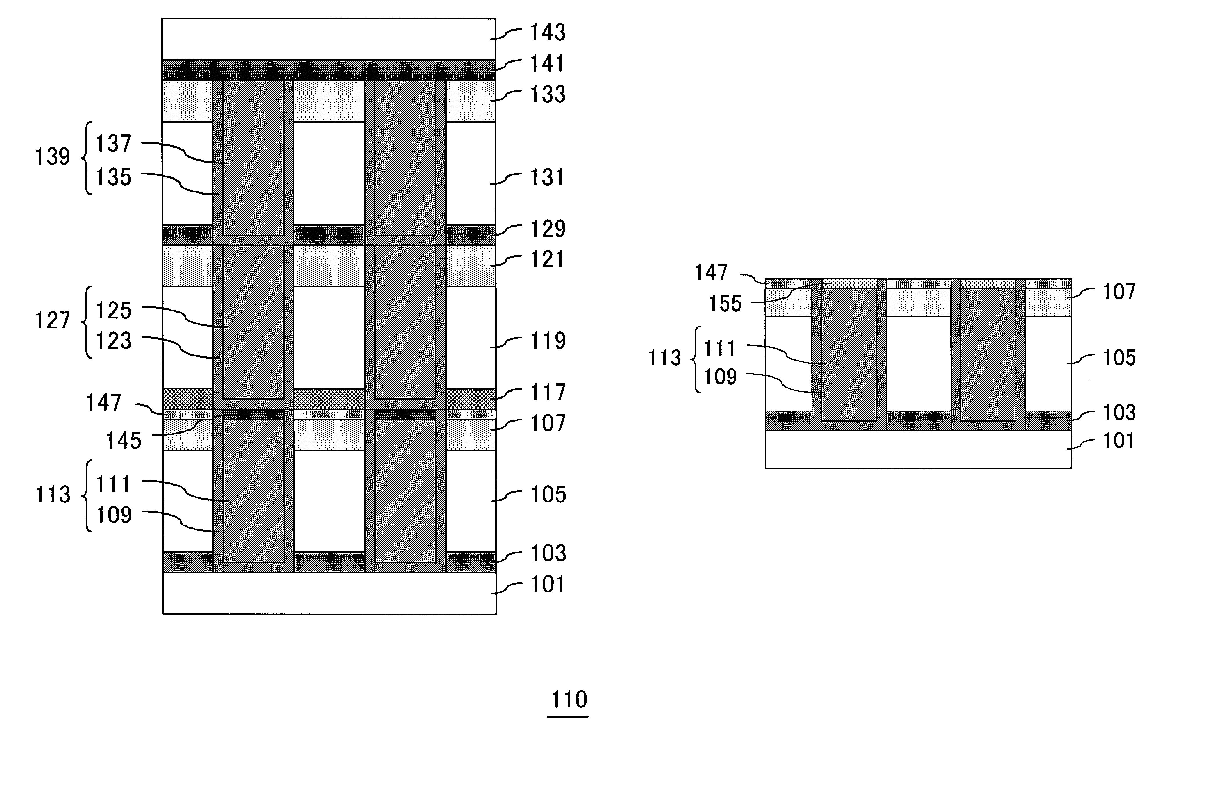
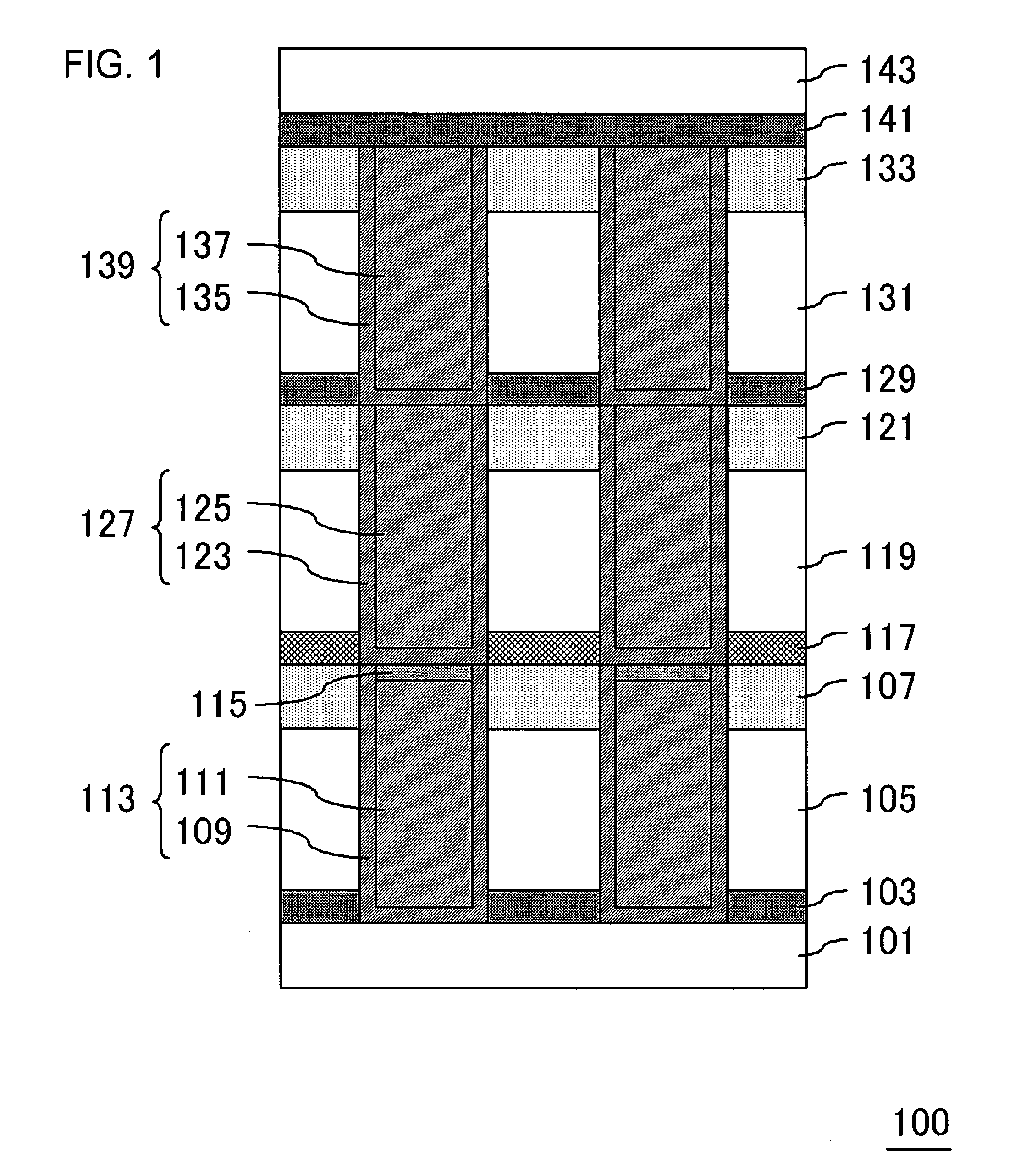
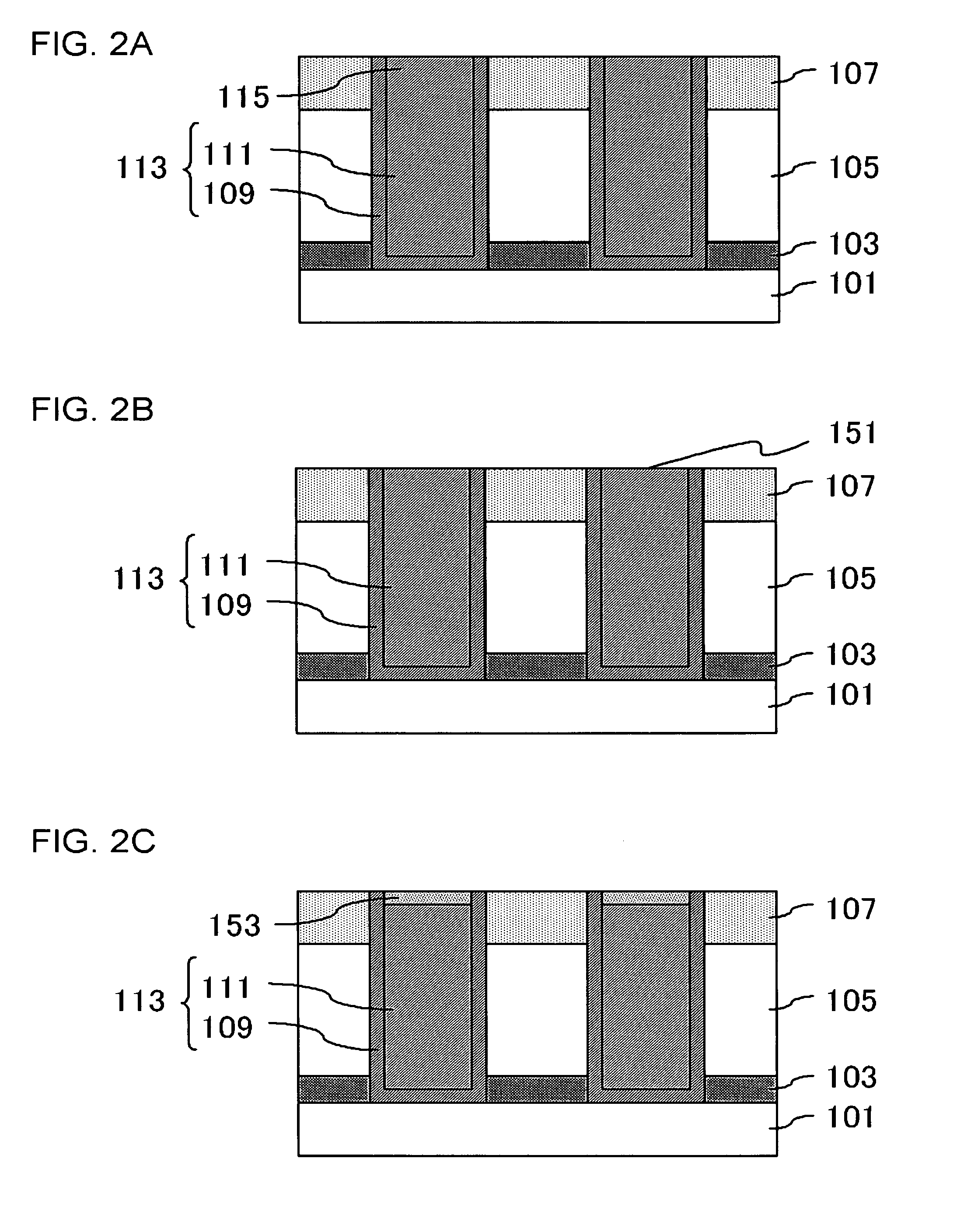
[0047]FIG. 1 is a cross-sectional view, illustrating a configuration of a semiconductor device of the present embodiment. A semiconductor device 100 shown in FIG. 1 includes a substrate such as a semiconductor substrate (a silicon substrate 101), a first insulating film (an SiCN film 103, an SiOC film 105 and an SiO2 film 107) provided on the silicon substrate 101, and an interconnect (a first copper interconnect 111) provided in the first insulating film and essentially composed of a copper-containing metal. Further, the semiconductor device 100 has a region doped with injected silicon (an Si unevenly distributed layer 153 of FIG. 2C) in the vicinity of the surface in the inside of the first copper interconnect 111, and injected atomic silicon at least partially creates Si—O bond (Si—O unevenly distributed layer 115).

[0048]Here, in the following descriptions of the present and the other embodiments, “in the vicinity of the surface of the interconnect in the inside thereof” means in...

second embodiment

[0091]While the SiC film 117 is formed on the first copper interconnect 111 after oxidation of silicon injected in the first copper interconnect 111 is conducted in the first embodiment, the procedure may also be conducted with reverse sequential order. In the present embodiment, a procedure in manufacturing the semiconductor device 100 will be described, which includes: injecting silicon in the first copper interconnect 111, and then first forming the SiC film 117, and thereafter oxidizing silicon injected in the first copper interconnect 111.

[0092]A manufacturing process of the present embodiment includes an operation (step 19) for forming the second insulating film so as to be in contact with the first insulating film having the first copper interconnect 111 formed therein, after the step 14 for injecting silicon and before the step 15 for creating Si—O bond. The second insulating film may be, for example, a film described in the first embodiment. In the present embodiment, the S...

third embodiment

[0098]While the configuration that silicon in the Si unevenly distributed layer 153 forms Si—O bond is illustrated in the first embodiment, silicon in the Si unevenly distributed layer 153 may form Si—O bond or Si—N bond.

[0099]FIG. 5 is a cross-sectional view, illustrating configuration of such type of semiconductor device. Fundamental configurations of the semiconductor device 110 shown in FIG. 5 are similar to that of the semiconductor device 100 shown in FIG. 1, except that silicon injected in the vicinity of the surface in the inside of the first copper interconnect 111 at least partially forms Si—N bond in the semiconductor device 110. Further, in the semiconductor device 110, Si—N bond is present in the vicinity of the surface in the inside of the SiO2 film 107.

[0100]More specifically, in the semiconductor device 110, an Si—O and Si—N unevenly distributed layer 145 is formed in the vicinity of the surface in the inside of the first copper interconnect 111. The Si—O and Si—N un...


PUM

PropertyMeasurementUnit
thicknessaaaaaaaaaa
specific dielectric constantaaaaaaaaaa
thicknessaaaaaaaaaa

Abstract

An improved migration resistance of the interconnect is provided and a diffusion of silicon into the inside of the interconnect is suppressed. A semiconductor device includes a silicon substrate, a first insulating film provided on the silicon substrate and composed of an SiCN film, an SiOC film and an SiO2 film, and a first copper interconnect provided in the first insulating film and essentially composed of a copper-containing metal. An Si—O unevenly distributed layer doped with injected silicon is included in the vicinity of the surface in the inside of the first copper interconnect, and injected atomic silicon at least partially creates Si—O bond.

Description

[0001]This application is based on Japanese patent application No. 2006-28,308, the content of which is incorporated hereinto by reference.BACKGROUND[0002]1. Technical Field[0003]The present invention relates to a semiconductor device and a method for manufacturing thereof, and particularly relates to a semiconductor device, which comprises an interconnect containing a copper-containing metal and a method for manufacturing thereof.[0004]2. Related Art[0005]In recent years, requirements in increasing operation speed of semiconductor devices promotes application of lower resistive materials such as copper and the like for interconnect materials. When a copper-containing metal is employed for an interconnect material, a barrier insulating film for preventing a diffusion of copper (Cu) is provided in a lower layer of an insulating interlayer.[0006]Meanwhile, as the level of the miniaturization of the semiconductor device is progressed, a signal delay due to an increased parasitic capaci...

Claims


Application Information

Patent Timeline
Patent Type & Authority Patents(United States)
IPC IPC(8): H01L23/48
CPCH01L21/76832H01L21/76834H01L21/76838H01L23/53238H01L2924/0002H01L2924/00
Inventor USAMI, TATSUYAOHTO, KOICHI
Owner RENESAS ELECTRONICS CORP
Why Eureka
Try Eureka