

Frame pulse signal latch circuit and phase adjustment method
a latch circuit and frame pulse technology, applied in the direction of synchronisation signal speed/phase control, digital transmission, transmission, etc., can solve the problems of long time required for designing and adjusting devices, the design of printed wiring boards of latch circuits is generally difficult, and the latch circuit cannot generate the frame pulse signal having the original cycle. , to achieve the effect of reliable latching of frame pulse signals, shortening the time taken, and shortening the length of printed wiring boards
- Summary
- Abstract
- Description
- Claims
- Application Information
AI Technical Summary
Benefits of technology
Problems solved by technology
Method used
Image

Examples
first embodiment
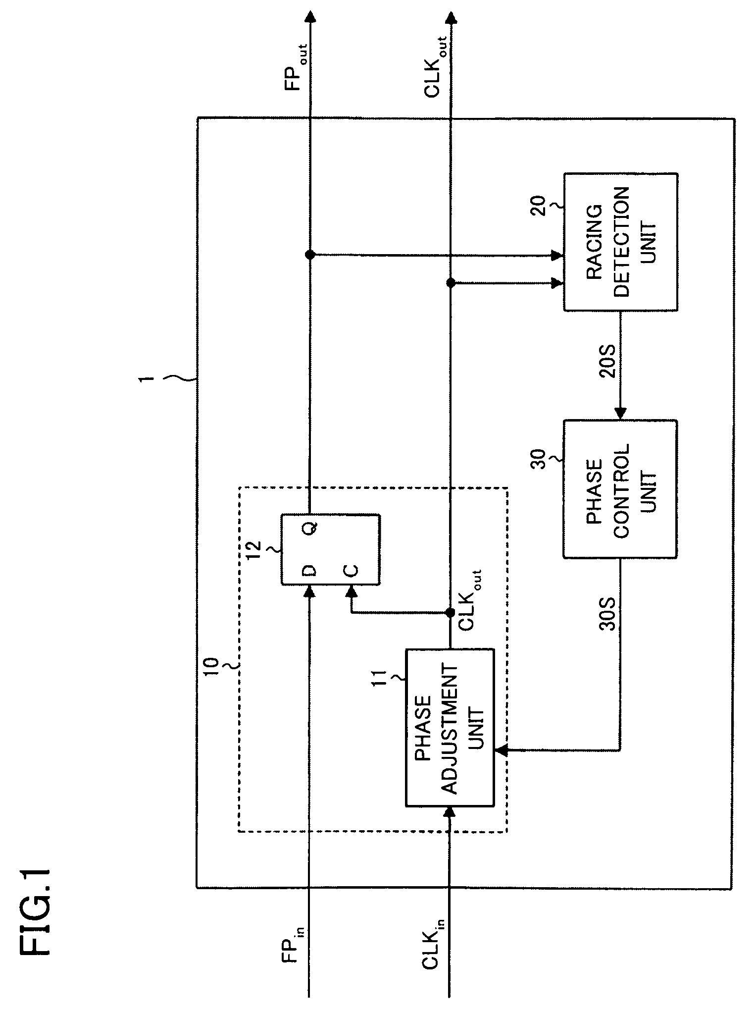
[0025]First, with reference to FIG. 1, a frame pulse signal latch circuit 1 according to a first embodiment of the present invention will be explained. FIG. 1 is a block diagram showing a configuration of the frame pulse signal latch circuit 1 according to the first embodiment of the present invention.
[0026]The frame pulse signal latch circuit 1 according to the present embodiment is a device, which latches an input frame pulse signal FPin at optimal timing based on an output clock signal CLKout obtained by adjusting the phase of an input clock signal CLKin. The frame pulse signal latch circuit 1 has a phase adjustment circuit 10, a racing detection unit 20, and a phase control unit 30.
[0027]The phase adjustment circuit 10 has a phase adjustment unit 11 and a latch unit 12. The phase adjustment unit 11 adjusts the phase of the input clock signal CLKin based on a signal 30S, which is output from the phase control unit 30, and outputs the signal as the output clock signal CLKout. The ...
second embodiment
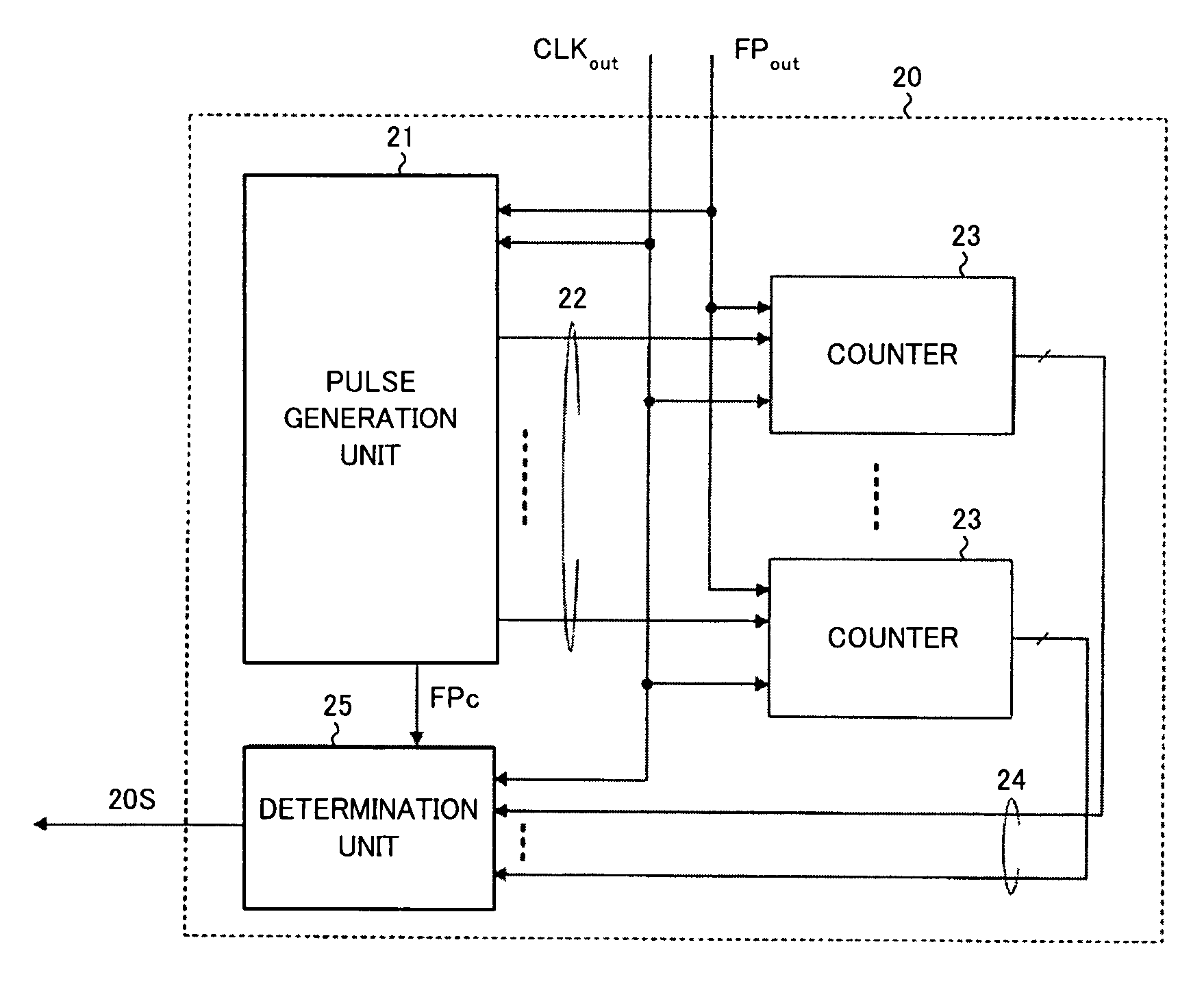
[0046]Next, a frame pulse signal latch circuit 1 according to a second embodiment of the present invention will be explained with reference to FIG. 4. FIG. 4 is a block diagram showing a configuration of a racing detection unit 20 of the frame pulse signal latch circuit 1 according to the second embodiment of the present invention.
[0047]In the present embodiment, a specific example of the racing detection unit 20 will be explained. Other configurations of the frame pulse signal latch circuit 1 are similar to that of the first embodiment. Therefore, detailed explanations thereof are omitted here.
[0048]As shown in FIG. 4, the racing detection unit 20 has a pulse generation unit 21, a plurality of counters 23, and a determination unit 25.
[0049]The pulse generation unit 21 counts the number of pulses of the output clock signal CLKout over one cycle of the output frame pulse signal FPout output from the latch unit 12. Then, based on the counted result, the pulse generation unit 21 genera...
third embodiment
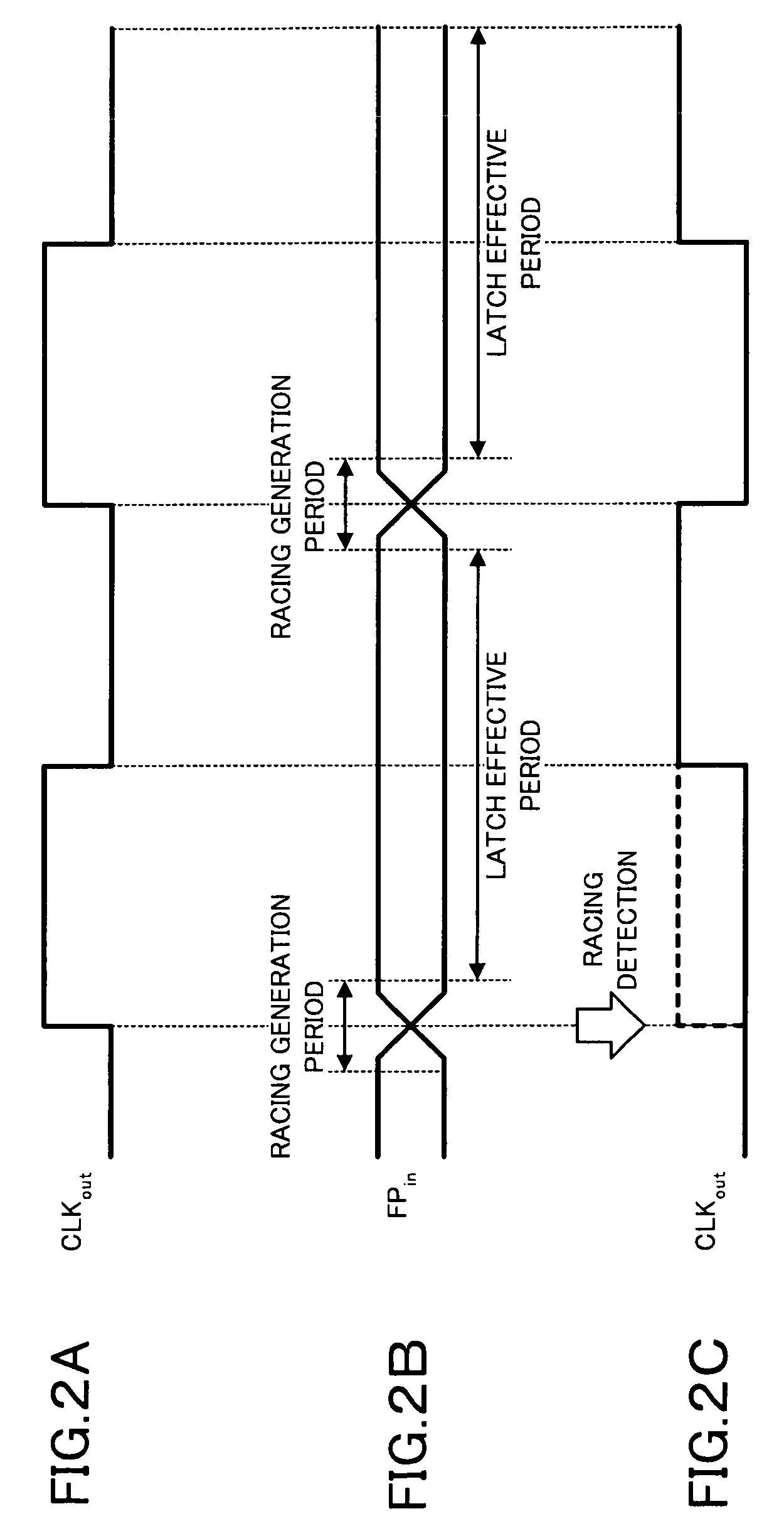
[0072]Next, with reference to FIG. 8 and FIG. 9A to FIG. 9I, a frame pulse signal latch circuit 1 according to a third embodiment of the present invention will be explained. FIG. 8 is a block diagram showing a configuration of the frame pulse signal latch circuit 1 according to the third embodiment of the present invention. Note that the configurations similar to the configurations shown in FIG. 4 are denoted by the same reference numerals. FIG. 9A to FIG. 9I are timing charts for explaining operations of the frame pulse signal latch circuit according to the third embodiment of the present invention.
[0073]In the present embodiment, in a case which will be explained, in the racing detection unit 20 according to the second embodiment, the racing state is detected by using a pulse signal 22A, which becomes the high level approximately at the same time when the input frame pulse signal FPin becomes the high level, and using a pulse signal 22B, of which phase is delayed by the period cor...
PUM
 Abstract
Description
Claims
Application Information