Solid-state imaging apparatus including pixel matrix with selectable blocks of output lines and imaging system using the solid-state imaging apparatus

a solid-state imaging and output line technology, applied in the direction of color television details, television system details, television systems, etc., can solve the problems of inability to read out the signals in the order in which the pixels are arrayed, the outputs of the ob pixels cannot be read out and the outputs of the ob pixels cannot be corrected from the output terminal on the right side using the ob pixels

Active Publication Date: 2012-12-04
CANON KK
View PDF35 Cites 38 Cited by
  • Summary
  • Abstract
  • Description
  • Claims
  • Application Information

AI Technical Summary

Benefits of technology

[0010]It is an object of the present invention to provide a solid-state imaging apparatus mounted with an analog-to-digital converter that can output digital signals at high speed and can output the digital signals in order in which the pixels are arrayed and an imaging system using the solid-state imaging apparatus. A solid-state imaging apparatus according to the present invention comprises: a pixel region including a plurality of pixels arranged in a matrix, wherein the pixel performs photoelectric conversion to output an analog signal; a plurality of analog-to-digital converters for converting the analog signal into a digital signal arranged such that each of the analog-to-digital converters corresponds to each column of the pixels; a plurality of digital memories for holding the digital signal converted by the analog-to-digital converter; a plurality of block digital output lines arranged such that each one or more of the block digital output lines corresponds to each of blocks of the digital memories, wherein one of the blocks of the digital memories includes a plurality of the digital memories, and such that the digital signal held in a particular digital memory is output through the block digital output line corresponding to the block including the particular digital memory; a common digital output line for outputting the digital signal from the plurality of block digital output lines; a buffer circuit for buffering the digital signal from the block digital output line arranged between the block digital output line and the common digital output line; and a block selecting unit arranged between the block digital output lines and the common digital output line or between two adjacent block digital output lines, the block selecting unit being capable of switching the digital output lines to be electrically connected to the common digital output line or to an adjacent block digital output line.

Problems solved by technology

However, in the configuration disclosed in Japanese Patent Application Laid-Open No. 2008-103992, there is a significant problem in that, in the system for dividing the pixels into the left and right sections in the column direction of the pixels, signals cannot be read out in order in which the pixels are arrayed.
However, when the pixels are divided into the left and right sections, for example, if the OB pixels are arranged only on the left side of a pixel region, outputs of the OB pixels cannot be read out from an output terminal on the right side.
Therefore, it is difficult to correct the outputs read out from the output terminal on the right side using the OB pixels.

Method used


Image

  • Solid-state imaging apparatus including pixel matrix with selectable blocks of output lines and imaging system using the solid-state imaging apparatus
  • Solid-state imaging apparatus including pixel matrix with selectable blocks of output lines and imaging system using the solid-state imaging apparatus
  • Solid-state imaging apparatus including pixel matrix with selectable blocks of output lines and imaging system using the solid-state imaging apparatus

Examples


first embodiment

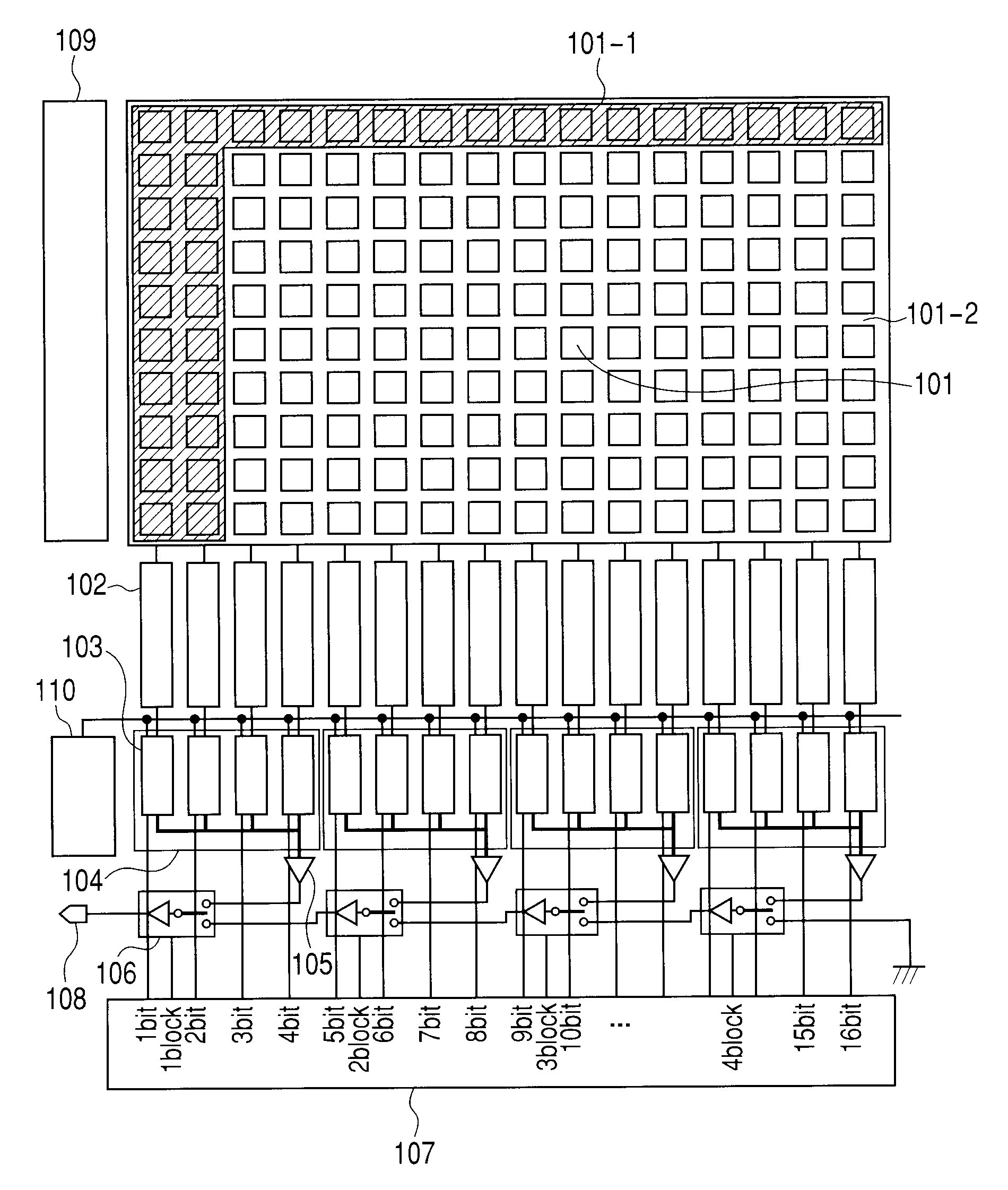
[0028]FIG. 1 is a diagram of a basic circuit configuration example of a MOS type solid-state imaging apparatus according to a first embodiment of the present invention. Basic circuits of this configuration example are formed on the same substrate of silicon and configured as one solid-state imaging apparatus. In this embodiment, for simplification, a pixel region is a pixel region 101 with pixels arranged in 10 rows×16 columns. One row at an upper end and two columns at a left end in this pixel region 101 are OB (optical black) pixels 101-1. Each of the OB pixels 101-1 has a photoelectric conversion element shielded from light. The other pixels in 9 rows×14 columns are effective pixels 101-2.

[0029]Reference numeral 102 denotes analog-to-digital converters (AD converters) provided to correspond to the columns of the pixel region 101. Reference numeral 103 denotes digital memories that temporarily store digital signals converted by the AD converters 102.

[0030]Reference numeral 104 den...

second embodiment

[0064]FIG. 7 is a block diagram illustrating a configuration example of a solid-state imaging apparatus according to a second embodiment of the present invention. In FIG. 7, since circuit units same as those in FIG. 1 are denoted by the same reference numerals, explanation of the circuit units is omitted. FIG. 8 is a timing chart illustrating readout timing in the second embodiment.

[0065]This embodiment is described in detail below with reference to the block diagram of FIG. 7 and the timing chart of FIG. 8. In this embodiment, two channels of common digital output lines 108 are present. Consequently, it is possible to simultaneously output digital signals from two columns, an even number column and an odd number column.

[0066]When the first bit is enabled, the horizontal scanning circuit 107 simultaneously performs read out from the digital memories 103 in the first column and the second column. In this embodiment, two channels of block digital output lines 104 and two channels of b...

third embodiment

[0074]FIG. 9 is a block diagram illustrating a configuration example of a solid-state imaging apparatus according to a third embodiment of the present invention. In FIG. 9, since circuit units same as those in FIG. 1 are denoted by the same reference numerals, explanation of the circuits is omitted. In this embodiment, the block digital output lines 104 are connected to the buffer circuits 105 via the block selecting units 106. Concerning timing for readout in this embodiment, signals can be read out at timing same as that in FIG. 6 described in the first embodiment. Therefore, detailed explanation of the timing is omitted.

[0075]In this embodiment, by providing the sense amplifier circuit illustrated in FIG. 4 in the buffer circuit 105, a differential format can be adopted for a format of a sense amplifier in the same manner as adopting the differential format for the output of the digital memory 103. As a result, it is easy to perform readout using the sense amplifier illustrated i...


PUM


Abstract

It is an object of the present invention to provide a solid-state imaging apparatus that outputs digital signals at high speed. A solid-state imaging apparatus is provided that includes plural analog-to-digital converters that convert analog signals obtained by photoelectric conversion into digital signals, plural digital memories that store the digital signals converted by the analog-to-digital converters, plural block digital output lines that are provided to correspond to blocks of the plural digital memories and to which the digital signals stored in the plural digital memories included in the blocks are output, a common digital output line that outputs the digital signals output from the plural block digital output lines, buffer circuits that buffer the digital signals output from the block digital output lines, and block selecting units that can switch the block digital output lines electrically connected to the common digital output line.

Description

BACKGROUND OF THE INVENTION[0001]1. Field of the Invention[0002]The present invention relates to a solid-state imaging apparatus including analog-to-digital converters (AD converters) and an imaging system using the solid-state imaging apparatus.[0003]2. Description of the Related Art[0004]In recent years, there is proposed a configuration for providing an AD converter for each of columns and performing high-speed readout in a MOS type solid-state imaging apparatus.[0005]FIG. 12 is a diagram illustrating the circuit configuration of a MOS type solid-state imaging apparatus 10 disclosed in Japanese Patent Application Laid-Open No. 2008-103992. Japanese Patent Application Laid-Open No. 2008-103992 discloses a solid-state imaging apparatus including AD converters 16 and 17 for each of columns of pixels 30 in order to realize an increase in speed. The solid-state imaging apparatus disclosed in Japanese Patent Application Laid-Open No. 2008-103992 includes plural data buses 19 and 20 tha...

Claims


Application Information

Patent Timeline
Patent Type & Authority Patents(United States)
IPC IPC(8): H04N3/14H04N5/335H04N5/217
CPCH04N5/3742H04N25/767
Inventor YAMAZAKIHIYAMA, HIROKIIWANE, MASAAKI
Owner CANON KK
Why Eureka
Try Eureka