Optimized multi-layer printing of electronics and displays

a multi-layer printing and display technology, applied in the field of electrical circuits, can solve the problems of inability to mount devices on internal layers, inability to produce well-defined features with good electrical properties, and insufficient approaches to date to achieve good electrical properties

Inactive Publication Date: 2012-12-18
CABOT CORP
View PDF429 Cites 27 Cited by
  • Summary
  • Abstract
  • Description
  • Claims
  • Application Information

AI Technical Summary

Problems solved by technology

However, low viscosity compositions are not as well developed as the high viscosity compositions.
Ink-jet printing of conductors has been explored, but the approaches to date have been inadequate for producing well-defined features with good electrical properties, particularly at relatively low temperatures.
In general, devices cannot be mounted on internal layers.

Method used


Image

  • Optimized multi-layer printing of electronics and displays
  • Optimized multi-layer printing of electronics and displays
  • Optimized multi-layer printing of electronics and displays

Examples


Embodiment Construction

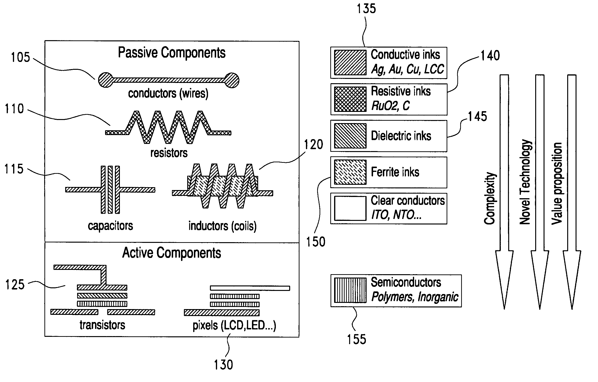
[0026]Digital printing of electronics using ink jet technology can enable the low cost production of circuits that today use expensive photolithography process. With ink jet printing, it will be possible to dramatically change the layout and construction method of these electronic circuits and also optimize materials usage by designing a new method and architecture for use of these electronic inks / materials.

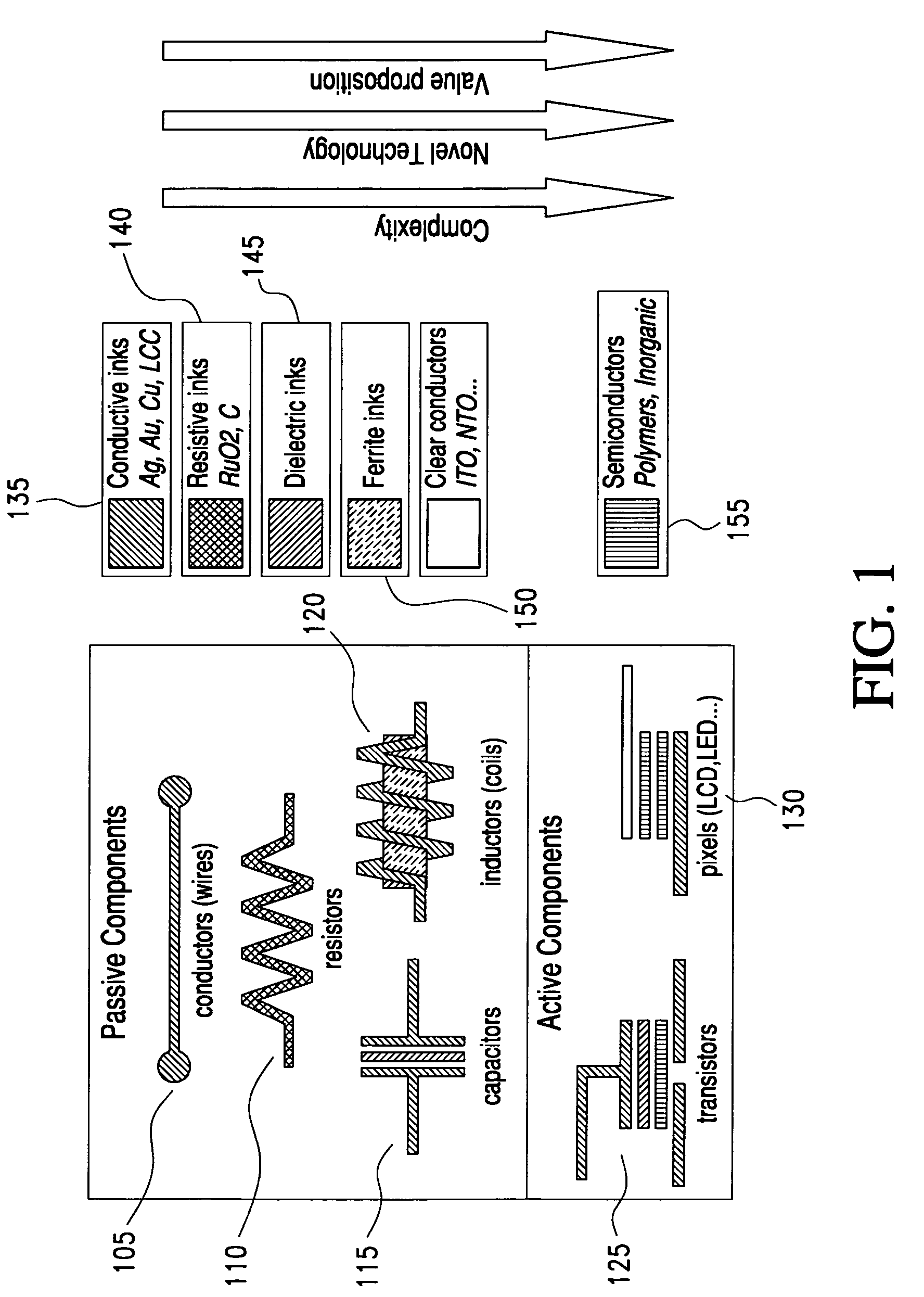
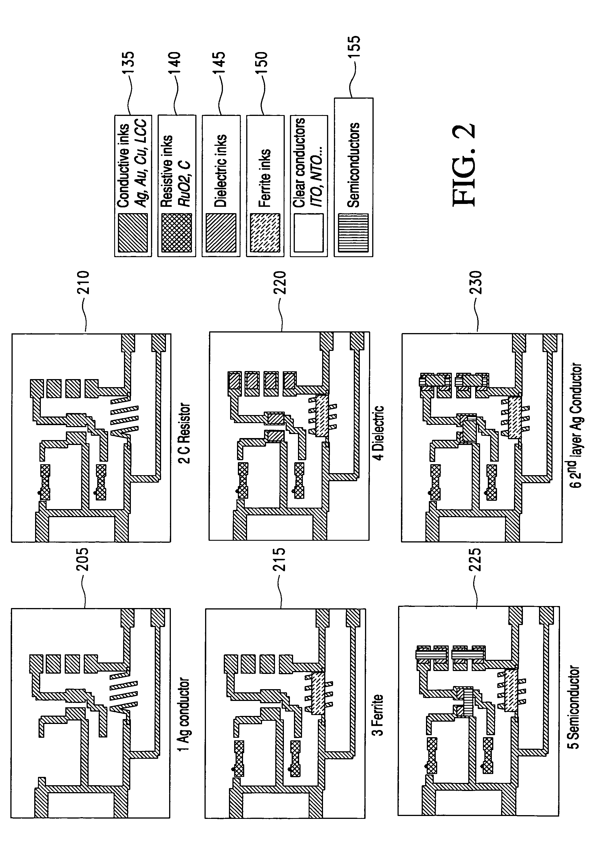
[0027]Referring to FIG. 1, the basic electronic components and materials that are used in producing printed circuit boards according to the present invention are illustrated. Passive components include a conductor 105 (i.e., a wire), a resistor 110, a capacitor 115, and an inductor 120. Active components include a transistor 125 and a pixel 130. Each of the passive components can be made using at least one out of five types of electronic inks: a conductive ink 135; a resistive ink 140; a dielectric ink or insulative ink 145; a ferrite ink 150; and a semiconductor ink 155. Insulat...


PUM

PropertyMeasurementUnit
dielectric constantaaaaaaaaaa
thicknessaaaaaaaaaa
viscosityaaaaaaaaaa

Abstract

An apparatus and method for making a printed circuit board comprising a substrate and an electrical circuit is provided. The circuit is formed by deposition of a plurality of electronic inks onto the substrate and curing of each of the electronic inks. The deposition may be performed using an ink-jet printing process. The inkjet printing process may include the step of printing a plurality of layers, wherein a first layer includes at least one electronic ink deposited directly onto the substrate, and wherein each subsequent layer includes at least one electronic ink deposited on top of at least a portion of a previous layer when the previous layer has been cured. One or more of the layers may include at least two of the electronic inks.

Description

CROSS-REFERENCE TO RELATED APPLICATIONS[0001]This application claims priority to U.S. Provisional Patent Application Ser. Nos. 60 / 643,577; 60 / 643,378; and 60 / 643,629, all filed on Jan. 14, 2005, the entireties of which are incorporated herein by reference. This application also claims priority to U.S. Provisional Patent Application Ser. No. 60 / 695,415, filed on Jul. 1, 2005, the entirety of which is incorporated herein by reference.STATEMENT REGARDING FEDERALLY-SPONSORED RESEARCH / DEVELOPMENT[0002]This invention was made with Government support under Agreement No. MDS972-93-2-0014 or DAAD19-02-3-0001 awarded by the Army Research Laboratory (“ARL”). The Government has certain rights in the invention.BACKGROUND OF THE INVENTION[0003]1. Field of the Invention[0004]The present invention relates to electrical circuits. More particularly, the invention relates to a method and apparatus for printing an electrical circuit onto a substrate using electronic inks that, when cured, have electric...

Claims


Application Information

Patent Timeline
Patent Type & Authority Patents(United States)
IPC IPC(8): H05K1/16
CPCH05K3/12H05K3/125H05K3/1275H05K1/16H05K1/095Y10T428/24917H05K3/1216H05K3/4664H05K2201/0326H05K2203/0113H05K2203/013H05K2203/0143H05K2203/0534H05K2203/1476Y10T428/24926
Inventor EDWARDS, CHUCKHOWARTH, JAMES JOHNVANHEUSDEN, KAREL
Owner CABOT CORP
Why Eureka
Try Eureka