Semiconductor memory device

a memory device and semiconductor technology, applied in the field can solve the problems of low power consumption of semiconductor memory devices, and achieve the effect of reducing bitline disturban

Active Publication Date: 2012-12-25
SAMSUNG ELECTRONICS CO LTD
View PDF9 Cites 380 Cited by
  • Summary
  • Abstract
  • Description
  • Claims
  • Application Information

AI Technical Summary

Benefits of technology

[0006]It is therefore a feature of an embodiment to provide a semiconductor memory device with reduced bitline disturbance.

Problems solved by technology

As the load capacitance on a dataline is increased, e.g., in order to increase the capacity of a semiconductor memory device, an operating voltage for a data accessing operation, such as a reading or writing operation, decreases, which leads to lower power consumption of the semiconductor memory device.

Method used


Image

  • Semiconductor memory device
  • Semiconductor memory device
  • Semiconductor memory device

Examples


Embodiment Construction

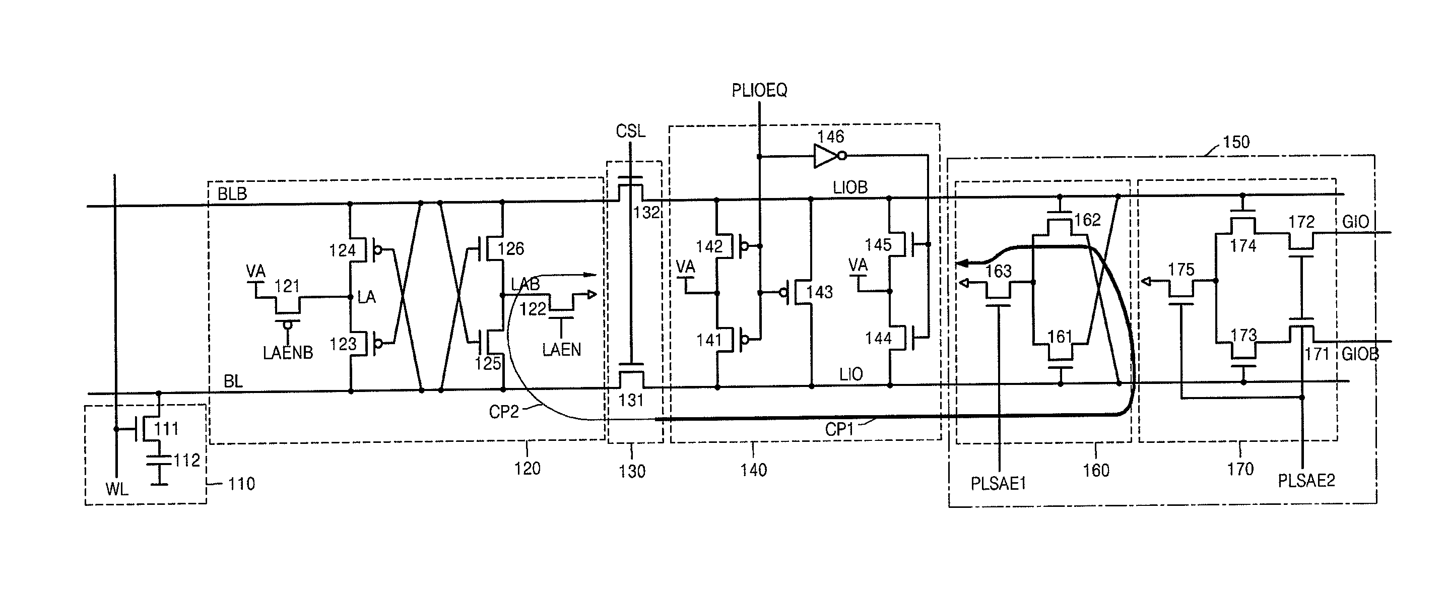
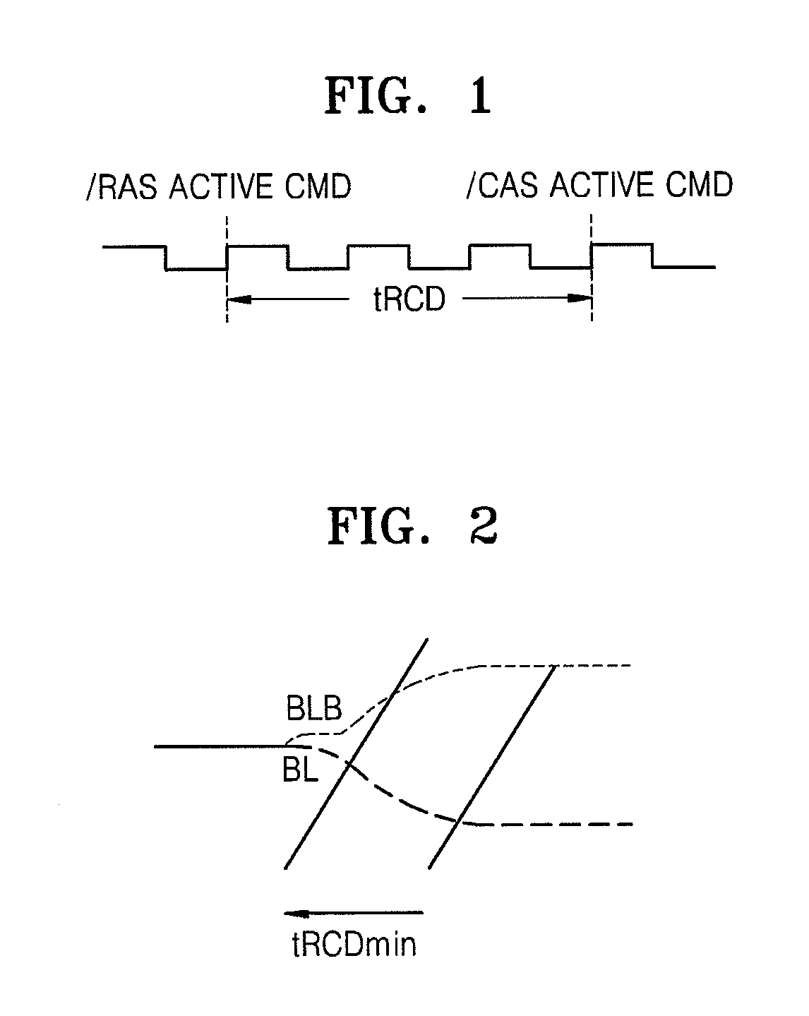
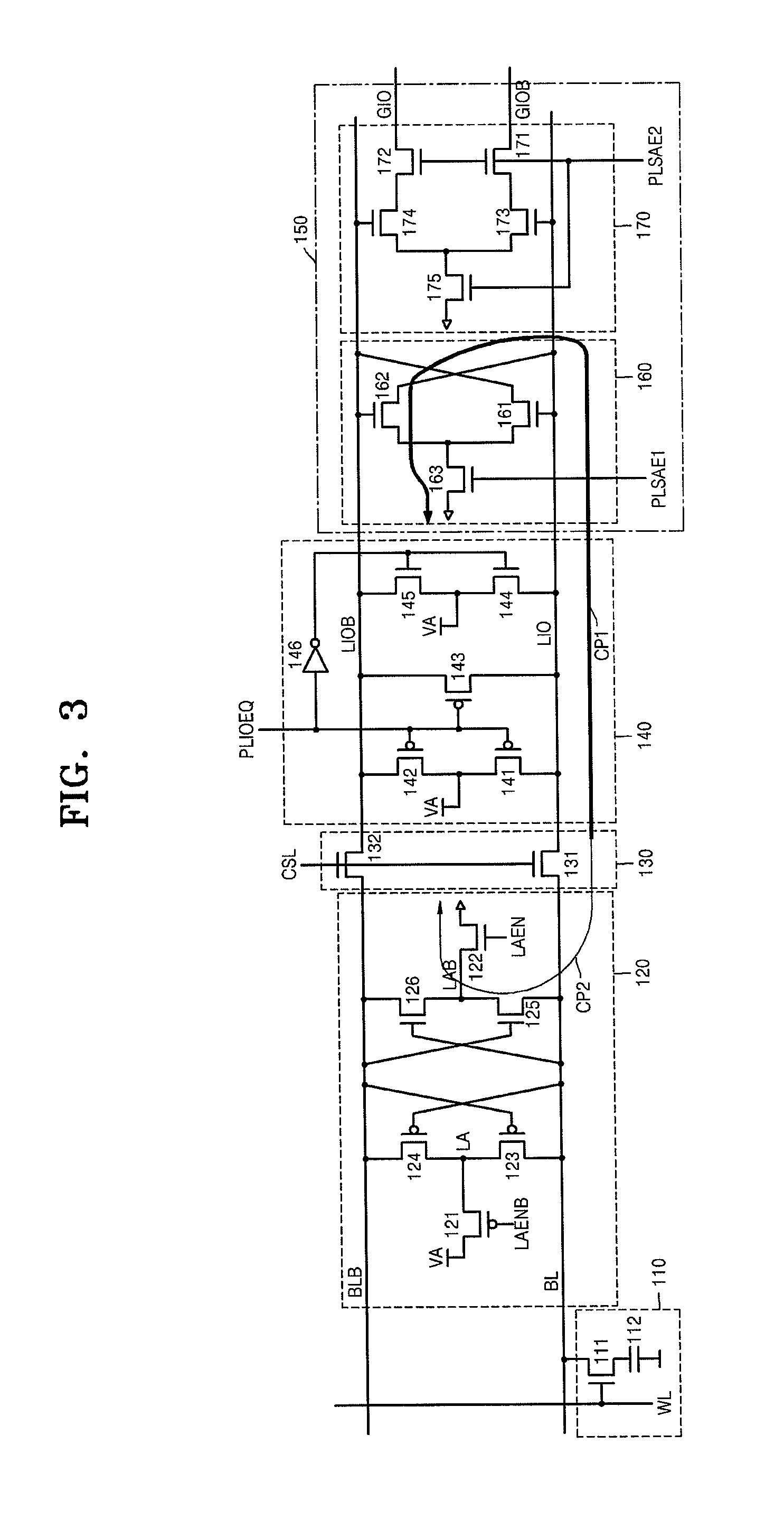
[0026]Korean Patent Application No. 10-2009-0111543, filed on Nov. 18, 2009, in the Korean Intellectual Property Office, and entitled: “Semiconductor Memory Device,” is incorporated by reference herein in its entirety.

[0027]Example embodiments will now be described more fully hereinafter with reference to the accompanying drawings; however, they may be embodied in different foams and should not be construed as limited to the embodiments set forth herein. Rather, these embodiments are provided so that this disclosure will be thorough and complete, and will fully convey the scope of the invention to those skilled in the art.

[0028]In the drawing figures, the dimensions of layers and regions may be exaggerated for clarity of illustration. It will also be understood that when a layer or element is referred to as being “on” another layer or substrate, it can be directly on the other layer or substrate, or intervening layers may also be present. Further, it will be understood that when a l...


PUM


Abstract

A semiconductor memory device includes a bitline sensing amp detecting and amplifying data of a pair of bitlines from a memory cell, a column selecting unit transmitting the data of the pair of bitlines to a pair of local datalines in response to a column selecting signal, a dataline precharging unit precharging the pair of local datalines to a precharging voltage level in response to a precharging signal, and a dataline sensing amp detecting and amplifying data transmitted to the pair of local datalines. The dataline sensing amp includes a charge sync unit discharging the pair of local datalines at the precharging voltage level in response to a first dataline sensing enabling signal and data of the pair of local datalines, and a data sensing unit transmitting data of the pair of local datalines to a pair of global datalines in response to a second dataline sensing enabling signal.

Description

BACKGROUND[0001]1. Field[0002]Embodiments relates to a semiconductor memory device, and more particularly, to a semiconductor memory device with reduced bitline disturbance and a method of operating the same.[0003]2. Description of the Related Art[0004]Nowadays, it is desirable to for semiconductor memory devices to have larger capacity, lower power consumption, and faster operational speed. As the load capacitance on a dataline is increased, e.g., in order to increase the capacity of a semiconductor memory device, an operating voltage for a data accessing operation, such as a reading or writing operation, decreases, which leads to lower power consumption of the semiconductor memory device. However, as the operating voltage level is lowered, the sensing margin for detecting and amplifying memory cell data may be reduced.SUMMARY[0005]Embodiments are therefore directed to semiconductor memory device, which substantially overcome one or more of the problems due to the limitations and d...

Claims


Application Information

Patent Timeline
Patent Type & Authority Patents(United States)
IPC IPC(8): G11C7/00
CPCG11C7/12G11C7/18G11C11/4094G11C11/4097G11C2207/002
Inventor YU, JE-MINKIM, BYUNG-CHULKIM, JUN-HYUNGHWANG, SANG-JOON
Owner SAMSUNG ELECTRONICS CO LTD
Why Eureka
Try Eureka