Non-linear capacitance compensation

a capacitance compensation and non-linear technology, applied in the direction of rf amplifiers, high-frequency amplifiers, gain control, etc., can solve the problems of significant linearity problems, spectral splatter or leakage of signal energy, and degradation of amplifier overall linearity

Active Publication Date: 2013-01-01
AVAGO TECH INT SALES PTE LTD
View PDF27 Cites 9 Cited by
  • Summary
  • Abstract
  • Description
  • Claims
  • Application Information

AI Technical Summary

Benefits of technology

[0008]Another aspect of the present invention is directed to a power amplifier that includes a gain stage and multiple compensation stages. The gain stage may include a pair of complementary amplifiers to receive a differential input signal and to output a differential amplified signal. In turn, each compensation stage has first and second compensation devices each coupled to an amplifier of one of the complementary amplifiers. In this way, each compensation device can compensate for a change in capacitance of the corresponding amplifier when the differential input signal is in a predetermined transition region of an input range. Such a power amplifier may be implemented in a wireless system to amplify signals provided by a transceiver or other such circuitry to an appropriate level for transmission via an antenna or other radiation means.

Problems solved by technology

AM-to-PM distortion is a non-linear process which degrades the amplifier's overall linearity.
These non-linear processes cause spectral splatter or leakage of signal energy from a desired channel to nearby channels.
However, in the case of highly efficient complementary metal oxide semiconductor (CMOS) power amplifiers, AM-to-PM distortion can cause a significant linearity problem.
AM-to-AM linearization techniques exist for CMOS devices, but such techniques either do not address AM-to-PM distortion, or they are rendered less effective because of AM-to-PM distortion.
As a result, an amplifier such as a power amplifier that is formed using CMOS devices can have linearity issues.
Class A) that improves the overall linearity but reduces the efficiency.

Method used


Image

  • Non-linear capacitance compensation
  • Non-linear capacitance compensation
  • Non-linear capacitance compensation

Examples


Embodiment Construction

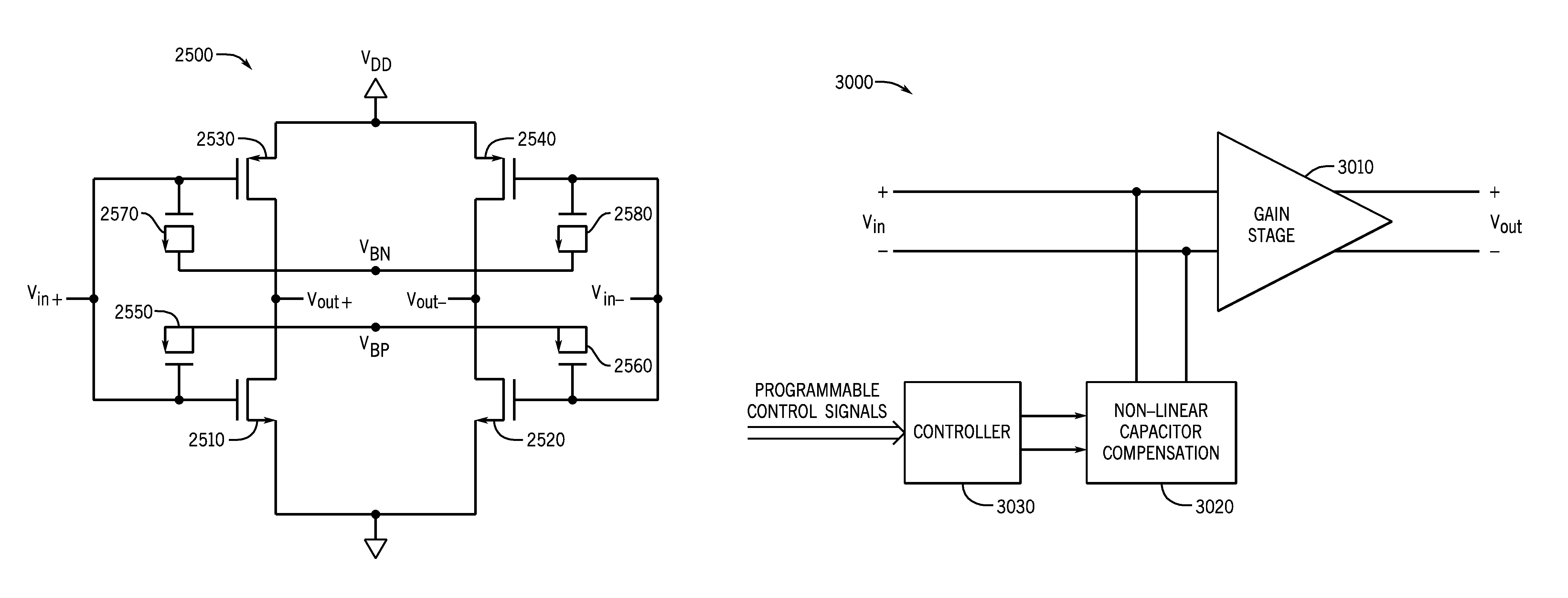
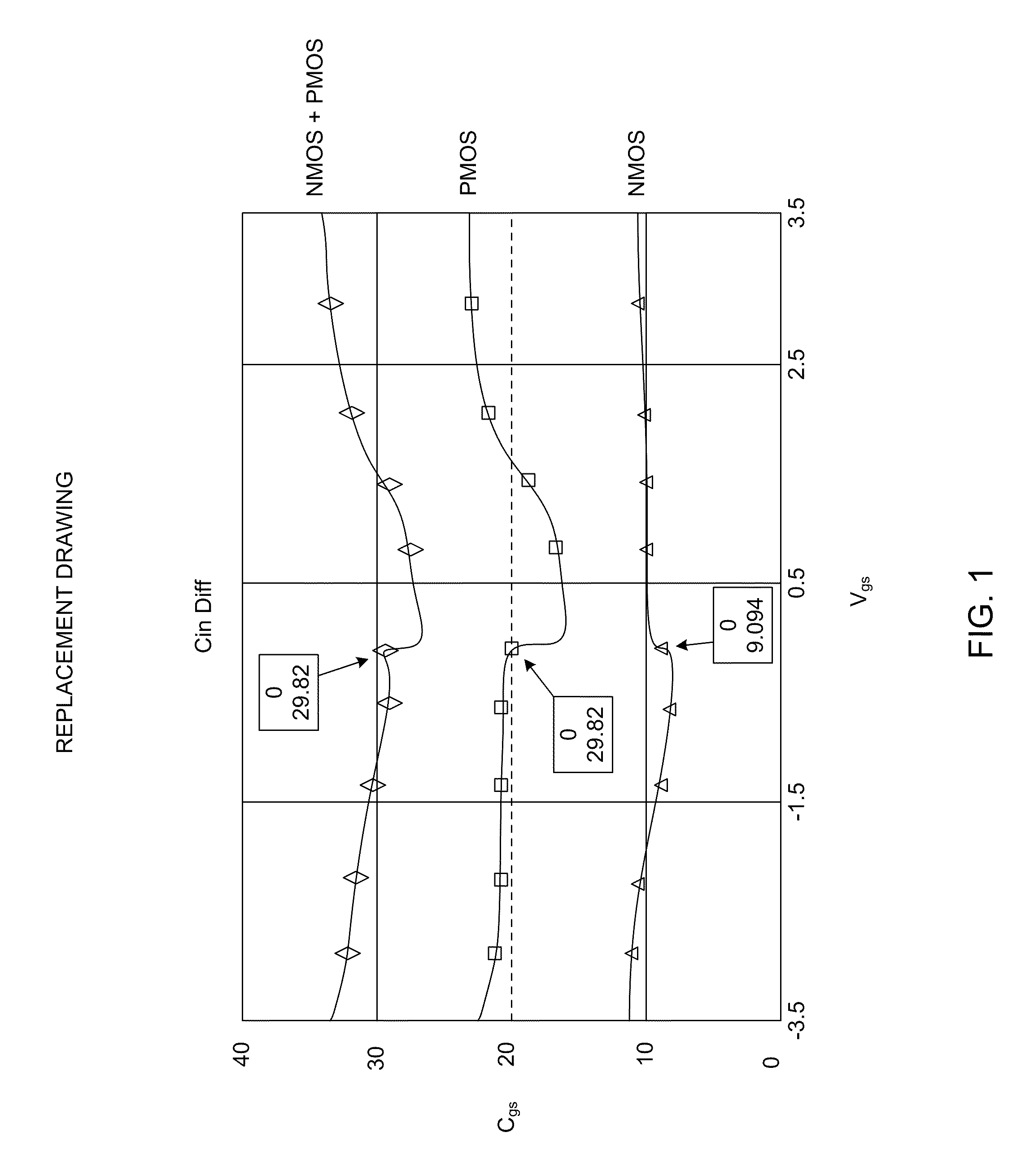
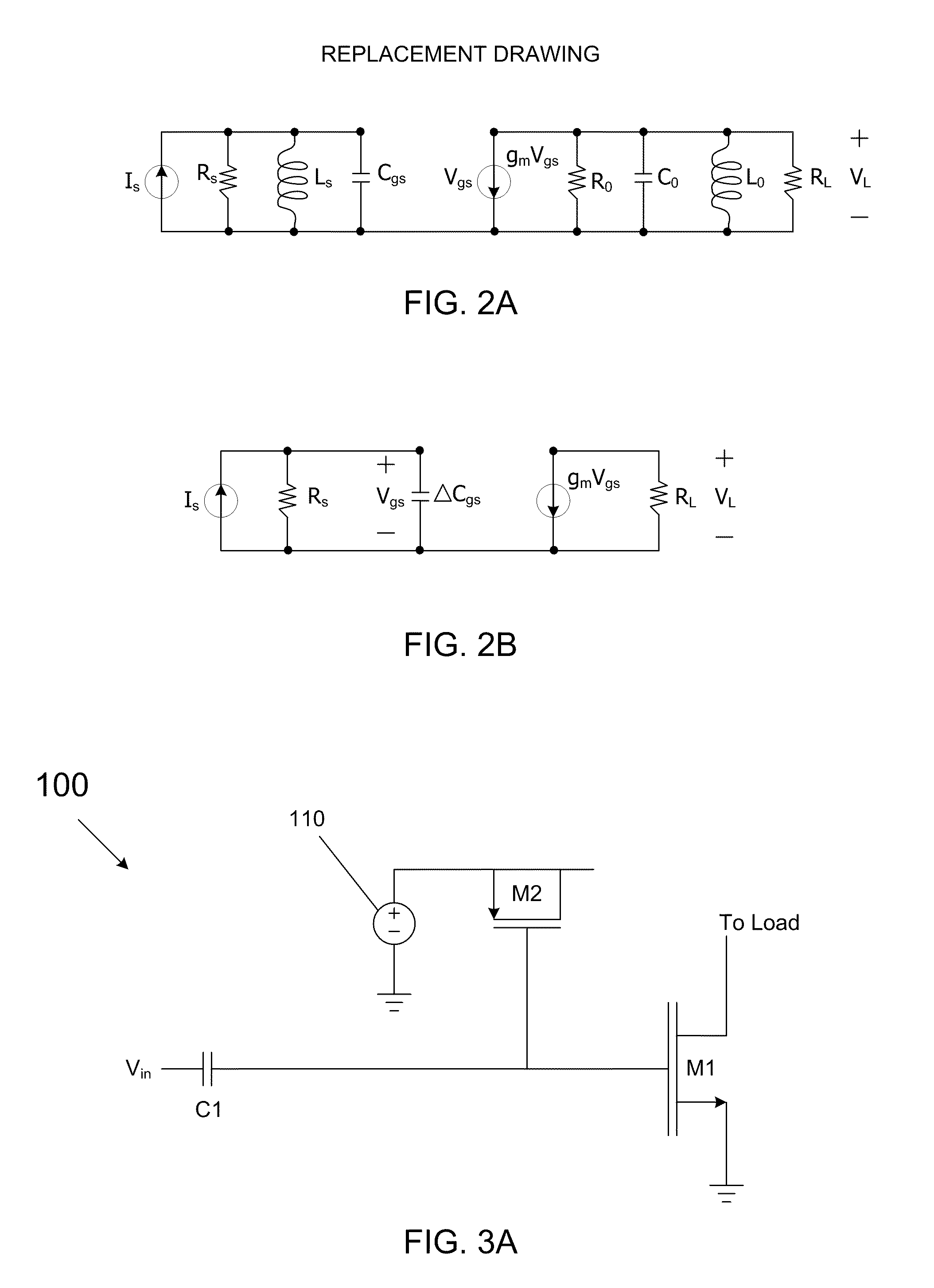
[0042]Embodiments may be used to improve linearity of an amplifier, and more particularly to improve phase linearity of a PA such as a CMOS PA. However, the techniques described herein may be used to improve linearity of CMOS devices in circuits beyond PAs. As will be described further below, embodiments may improve linearity by compensating for capacitance changes that occur to a device as it is provided with varying input signal levels. More specifically, as transistors dynamically change their characteristics when conducting in different operating regions, different inherent or parasitic capacitances may exist. Embodiments may attempt to reduce or remove the effects of such capacitance changes.

[0043]In a CMOS gain stage such as used in a PA, MOS devices can be configured as a complementary common-source amplifier in which multiple metal oxide semiconductor field effect transistors (MOSFETs), namely a p-channel MOSFET (PMOS) and an n-channel MOSFET (NMOS), are driven at the gates ...


PUM


Abstract

Embodiments are directed to capacitance compensation via a compensation device coupled to a gain device to compensate for a capacitance change occurring due to an input signal change, along with a controller coupled to the compensation device to receive the input signal and to control an amount of compensation based on the input signal. In some embodiments, banks may be formed of multiple compensation devices, where each of the banks has a different size and is coupled to receive a different set of bias voltages.

Description

[0001]This application is a continuation-in-part of U.S. patent application Ser. No. 12 / 080,066 entitled “COMPENSATION FOR NON-LINEAR CAPACITANCE EFFECTS IN A POWER AMPLIFIER,” filed on Mar. 31, 2008.BACKGROUND[0002]In various circuitry, amplifiers are commonly used to boost an amplitude of an incoming signal to a desired level. For example, various amplifiers may be present in a given system to boost signal strength of incoming signals to provide them at a desired level for further processing.[0003]In wireless systems such as cellular handsets, mobile internet devices, wireless personal digital systems (PDAs) and so forth, typically a power amplifier (PA) is present to receive a radio frequency (RF) signal modulated as desired for a given communication protocol and amplify this signal for transmission via an antenna of the device. Typically, a power amplifier can amplify both current and voltage of an incoming signal to provide the signal at a desired level.[0004]Different requirem...

Claims


Application Information

Patent Timeline
Patent Type & Authority Patents(United States)
IPC IPC(8): H03F1/14
CPCH03F1/086H03F1/14H03F3/19H03G3/00H03F3/3022H03F3/245H03F2200/451H03F2203/30144H03F3/45251
Inventor SAMAVEDAM, ANILBOCKELMAN, DAVID E.SRINIVASAN, VISHNUKIMBALL, ERIC
Owner AVAGO TECH INT SALES PTE LTD
Why Eureka
Try Eureka