Method for optimizing source and mask to control line width roughness and image log slope

a source and mask technology, applied in the field of integrated circuit pattern lithography, can solve the problems of limited resolution of lithographic tools, image distortion becomes a significant problem, and the biasing technique is ineffective to achieve the desired cds of the desired imag

Active Publication Date: 2013-02-12
GLOBALFOUNDRIES US INC
View PDF3 Cites 13 Cited by
  • Summary
  • Abstract
  • Description
  • Claims
  • Application Information

AI Technical Summary

Problems solved by technology

When the CD of desired lithographic patterns approaches the resolution limit of an optical lithography system, image distortions become a significant problem.
As the minimum CDs for semiconductor devices continue to decrease, the limited resolution of lithographic tools poses a challenge to improvements in IC manufacture.
However, in some situations geometric constraints that are inherent to the desired circuit pattern may require that the mask shapes be perturbed in opposite directions and / or contradictory positions.
In these situations, the biasing technique is ineffective to achieve the desired CDs of the desired image.
However, both “attenuated phase shift” and “alternating phase shift” techniques does not directly address the above-mentioned intrinsic geometric constraints in certain circuit patterns, though they do alleviate their severity by reducing image blur.
In addition, the “alternating phase shift” technique often adds unwanted features to image patterns.
For example, when opposite phases are applied to bright regions that pass in close proximity to one another at a certain point on the mask, the phase must make such an unwanted transition if the bright regions are connected together elsewhere in the mask pattern.
However, it is known that in practice the perimeter of printed circuit features will actually exhibit a fine-scale roughness whose fluctuations are typically sharper than the lens resolution.
LER becomes important for feature sizes of 100 nm or less, and can become a significant source of CD local uniformity control problems for features below 50 nm.

Method used


Image

  • Method for optimizing source and mask to control line width roughness and image log slope
  • Method for optimizing source and mask to control line width roughness and image log slope
  • Method for optimizing source and mask to control line width roughness and image log slope

Examples


Embodiment Construction

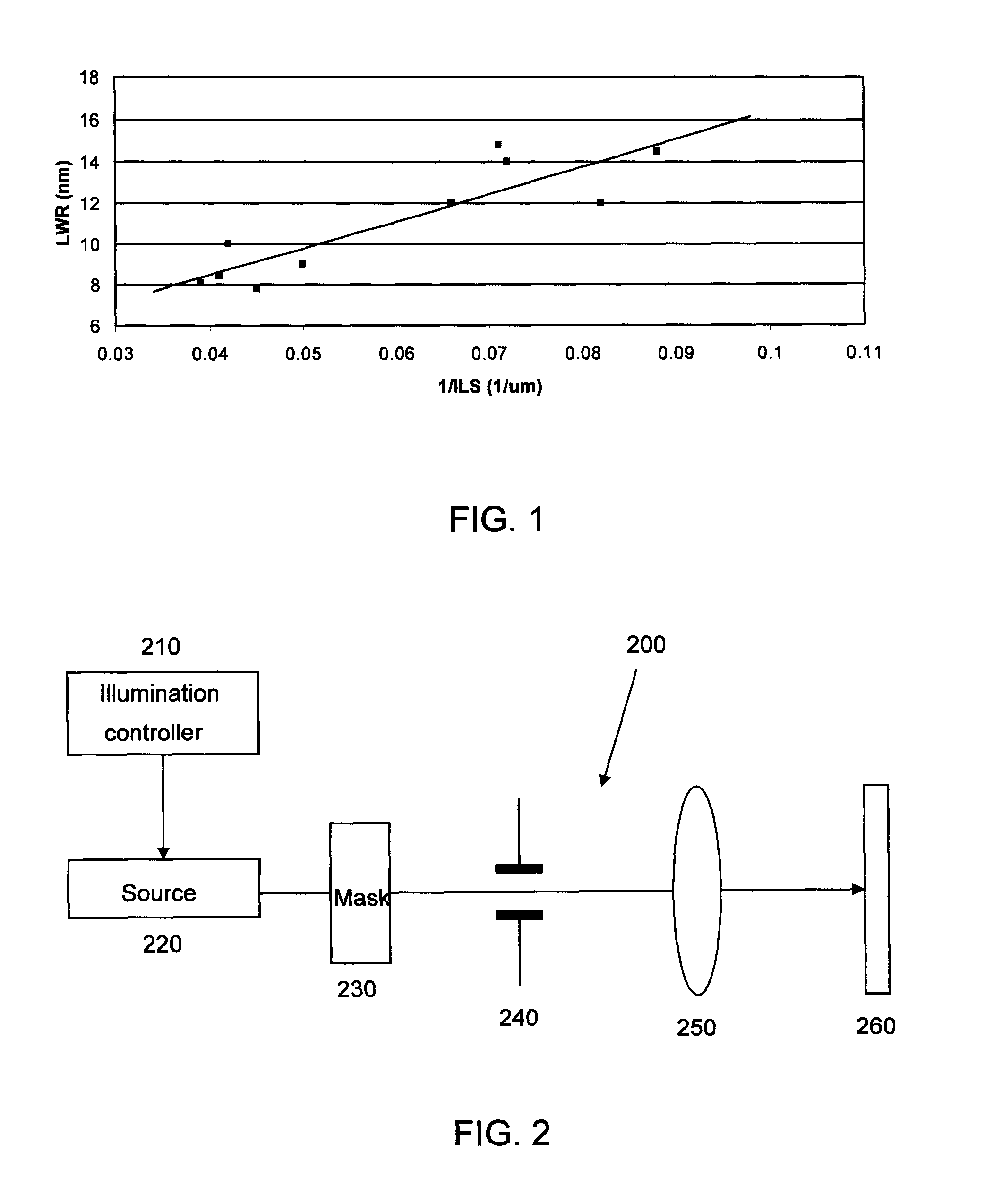
[0033]The various exemplary embodiments in accordance with this invention provide an improvement over conventional methods to reduce image distortions and improve image fidelity. This is accomplished by combining ways to optimize a lithographic image in a conventional SMO method with a new way of adjusting the image intensity to control LER.

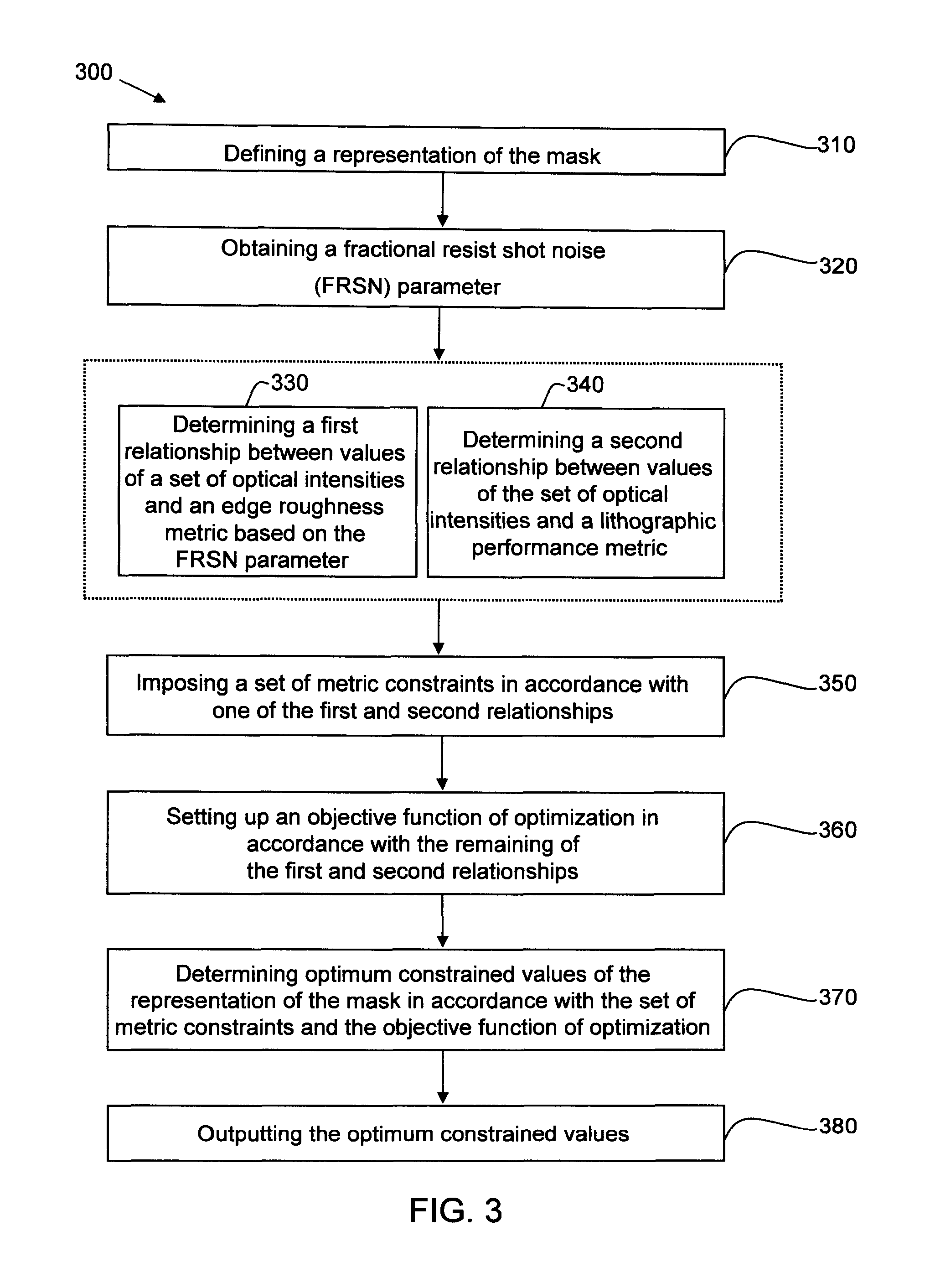
[0034]As used herein, a “source” or an “illumination source” refers to a device configured to emit radiation for the purpose of lithographic exposure.

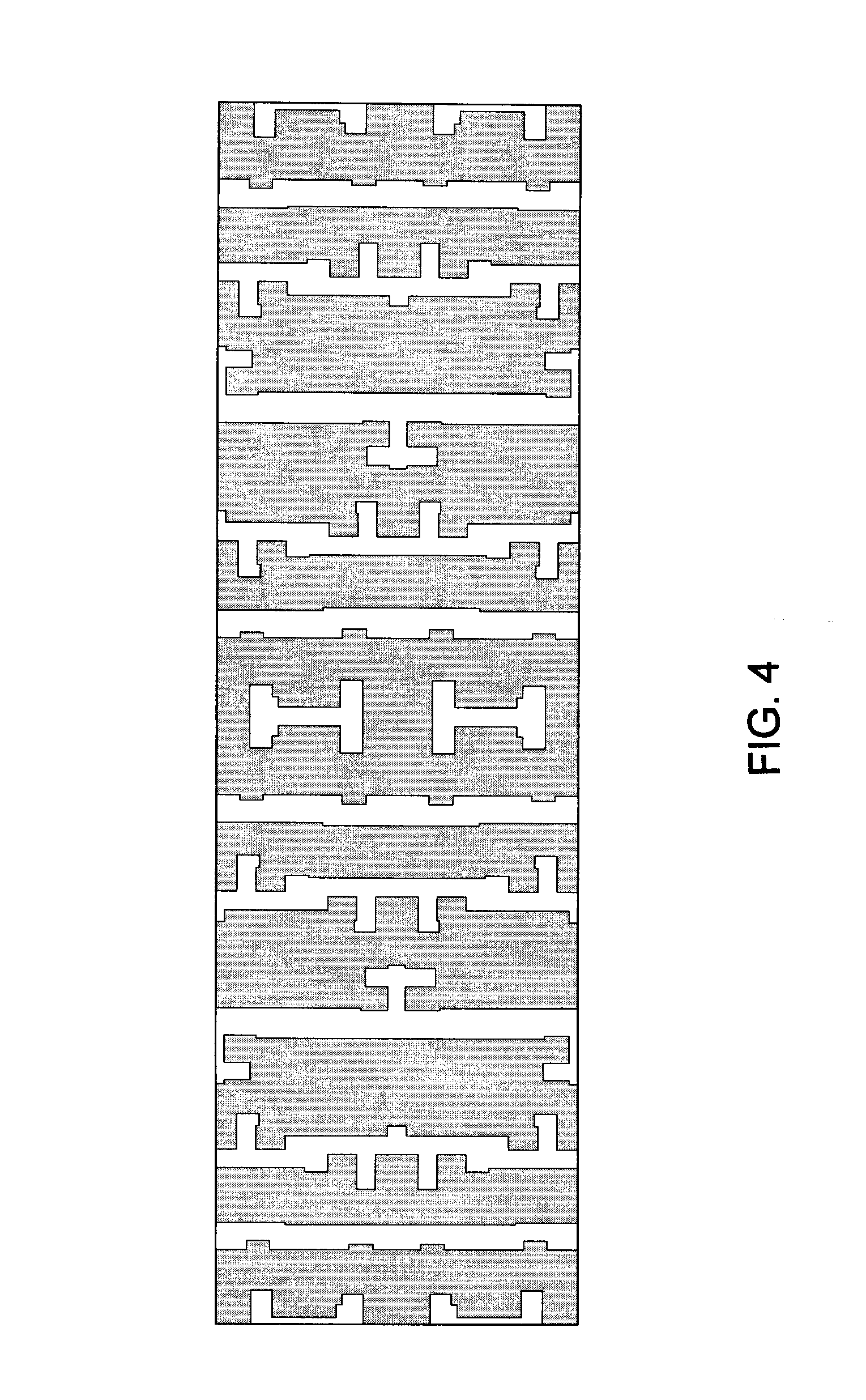
[0035]As used herein, a “mask” or a “lithography mask” refers to a template used in lithography that allows selective exposure of a photosensitive surface through a patterned layer included therein and having a different transparency than a background layer included therein.

[0036]In a conventional SMO method, the image relationships connect the image with standard lithographic metrics which assess sensitivity to defocus, dose control error, etc. In this method, the image intensity is a smoothly vary...


PUM

PropertyMeasurementUnit
feature sizesaaaaaaaaaa
lengthaaaaaaaaaa

Abstract

A method for illuminating a mask with a source to project a desired image pattern through a lithographic system onto a photoactive material including: defining a representation of the mask; obtaining a fractional resist shot noise (FRSN) parameter; determining a first relationship between a first set of optical intensity values and an edge roughness metric based on the FRSN parameter; determining a second relationship between a second set of optical intensity values and a lithographic performance metric; imposing a set of metric constraints based on one of the first and second relationships; setting up an objective function of optimization based on the remaining of the two relationships; determining optimum constrained values of the representation of the mask based on the set of metric constraints and the objective function; and outputting these values.

Description

FIELD OF THE INVENTION[0001]This invention relates generally to lithographic formation of integrated circuit patterns on a semiconductor chip, and more particularly to a method for selecting and using combinations of illumination source characteristics and diffracting shapes on a mask to form integrated circuit patterns on a semiconductor chip with controlled line width roughness and image log slope.BACKGROUND OF THE INVENTION[0002]Miniaturized electronic components such as integrated circuits (ICs) are typically manufactured using photolithography technology. In a photolithography process, a photoresist layer is formed on a semiconductor substrate, such as a silicon wafer. The photoresist layer is exposed through a photomask with a desired pattern to a source of actinic radiation. The radiation exposure causes a chemical reaction in the exposed areas of the photoresist and creates a latent image corresponding to the mask pattern in the photoresist layer. The photoresist is next dev...

Claims


Application Information

Patent Timeline
Patent Type & Authority Patents(United States)
IPC IPC(8): G03F9/00
CPCG03F1/70G03F7/70433
Inventor TIAN, KEHANROSENBLUTH, ALAN E.MELVILLE, DAVID O.AZPIROZ, JAIONE TIRAPUBAGHERI, SAEEDLAI, KAFAI
Owner GLOBALFOUNDRIES US INC
Why Eureka
Try Eureka