Electrical isolation of X-ray semiconductor imager pixels

a semiconductor imager and pixel technology, applied in the field of electromagnetic semiconductor detectors, can solve the problems of limiting the adoption of smaller pixel sizes, affecting the spectral resolution and count rate performance of detectors, so as to improve the count rate performance of semiconductor detectors, k-escape, and mitigate the negative effect of charge sharing on spectral resolution and count rate performan

Inactive Publication Date: 2013-02-12
KONINK PHILIPS ELECTRONICS NV
View PDF17 Cites 0 Cited by
  • Summary
  • Abstract
  • Description
  • Claims
  • Application Information

AI Technical Summary

Benefits of technology

[0005]In one embodiment, it is advantageous to mitigate the negative effect caused by charge sharing and thereby improve the spectral resolution and count rate performance of semiconductor detectors.
[0006]In one embodiment, it is advantageous to mitigate, or even eliminate the K-escape phenomenon of semiconductor detectors and thereby improve the count rate performance of semiconductor detectors.
[0007]In one embodiment, it is advantageous to mitigate the negative effect of charge sharing and K-escape on the miniaturization of pixel sizes of semiconductor detectors.
[0008]In a first aspect, according to one embodiment of the invention, a semiconductor detector is provided, comprising: a plurality of anodes arranged to form at least one opening, each opening being formed by two anodes in the plurality of anodes; at least one cathode; a detector cell located between the plurality of anodes and the at least one cathode; wherein the detector cell comprises at least one groove, each of the at least one groove having a first opening aligned with one of the at least one opening being formed by two anodes in the plurality of anodes, each of the at least one groove extending towards the at least one cathode. Forming one or more grooves in the detector cell is efficient to guide the charge cloud generated by a single photon received by a corresponding anode, instead of being received by several neighboring anodes. This provides the advantage of mitigating the negative effect of charge sharing on spectral resolution and count rate performance.
[0010]In another embodiment, each groove extends along a direction away from a direction which is perpendicular to the plane of its first opening. In other words, the direction of extension of the groove is inclined instead of being perpendicular to the tangential plane of a corresponding opening formed by two corresponding adjacent anodes. This shape is advantageous in that it decreases the phenomenon of reducing DQE (Detector Quantum Efficiency) of detectors.
[0011]In a second aspect, according to one embodiment of the invention, each groove comprises an insulator which is helpful in mitigating, or even eliminating, the negative effect of the K-escape phenomenon. It is preferred to use insulator with a high atomic number Z.

Problems solved by technology

However, these direct conversion materials are vulnerable because of charge sharing, a phenomenon in which the charge cloud generated by a single photon is collected by several neighboring electrodes. FIG. 1 shows that a charge cloud generated by one photon is collected by three neighboring electrodes.
The phenomenon of charge sharing disturbs the spectral resolution and count rate performance of detectors.
At the same time, the phenomenon of K-escape also limits the adoption of smaller pixel sizes.

Method used


Image

  • Electrical isolation of X-ray semiconductor imager pixels
  • Electrical isolation of X-ray semiconductor imager pixels
  • Electrical isolation of X-ray semiconductor imager pixels

Examples


Embodiment Construction

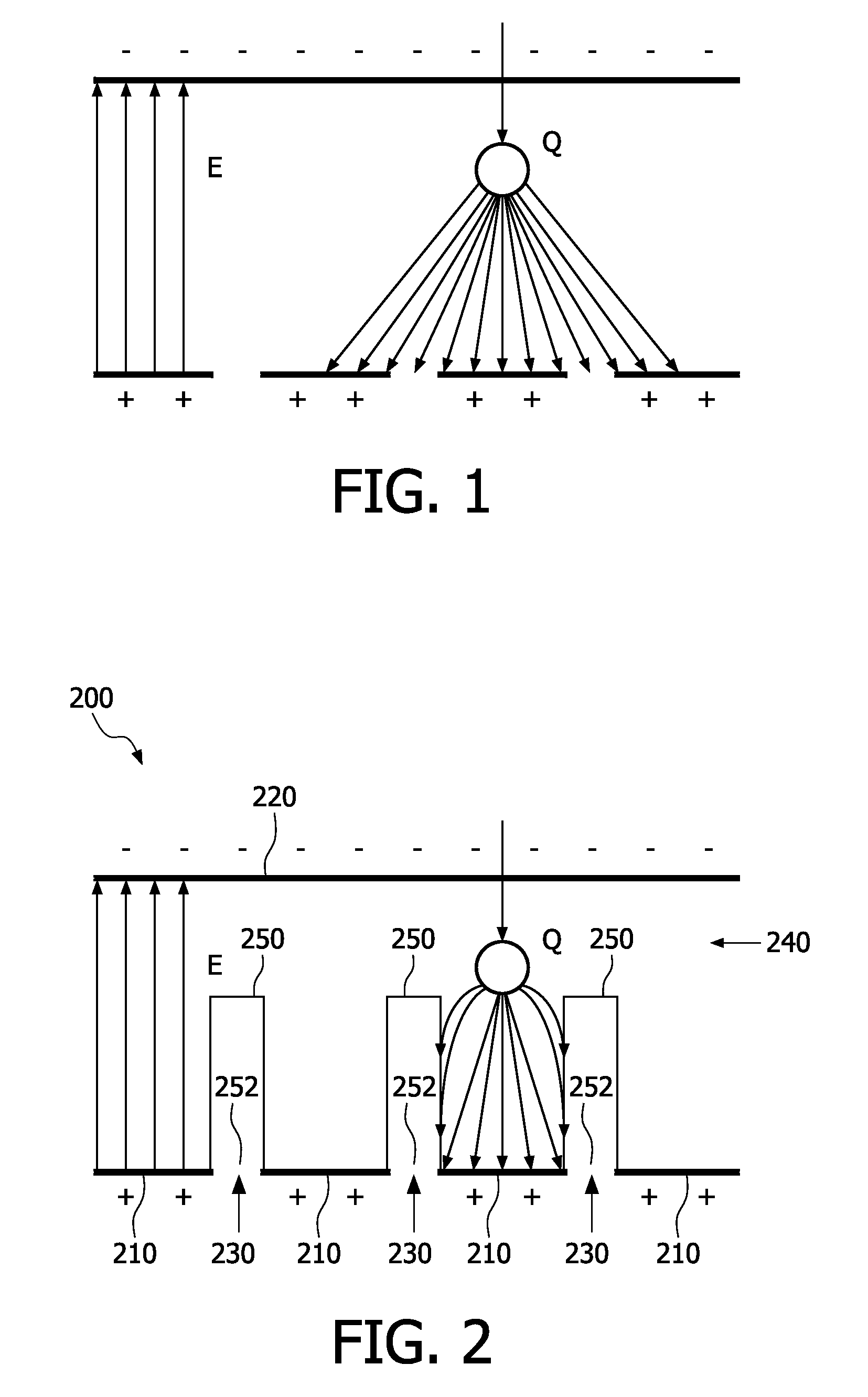
[0017]An embodiment of a structured semiconductor detector which mitigates or overcomes the drawback of the charge sharing effect in current semiconductor detectors is shown in FIG. 2. The detector 200 comprises a plurality of anodes 210, at least one cathode 220, and a detector cell 240. The anodes and the at least one cathode can be arranged in parallel, or in another configuration. Every two adjacent anodes form an opening 230. From each opening, a groove 250 extends into the detector cell 240, with its direction perpendicular to the plane of the opening 230. Each groove 250 has a first opening 252, which may have the same width as the corresponding opening 230, or which may be larger / smaller than the corresponding opening 230. It can clearly be seen that, due to the existence of grooves, a charge cloud generated by a photon is received by one corresponding anode instead of by two or more adjacent anodes.

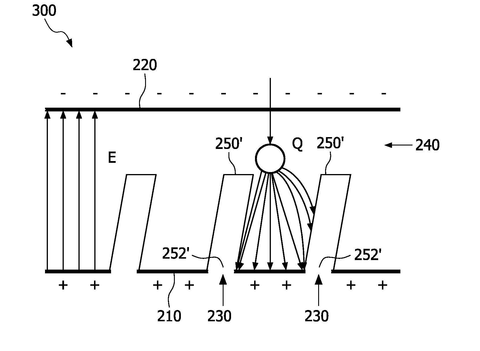
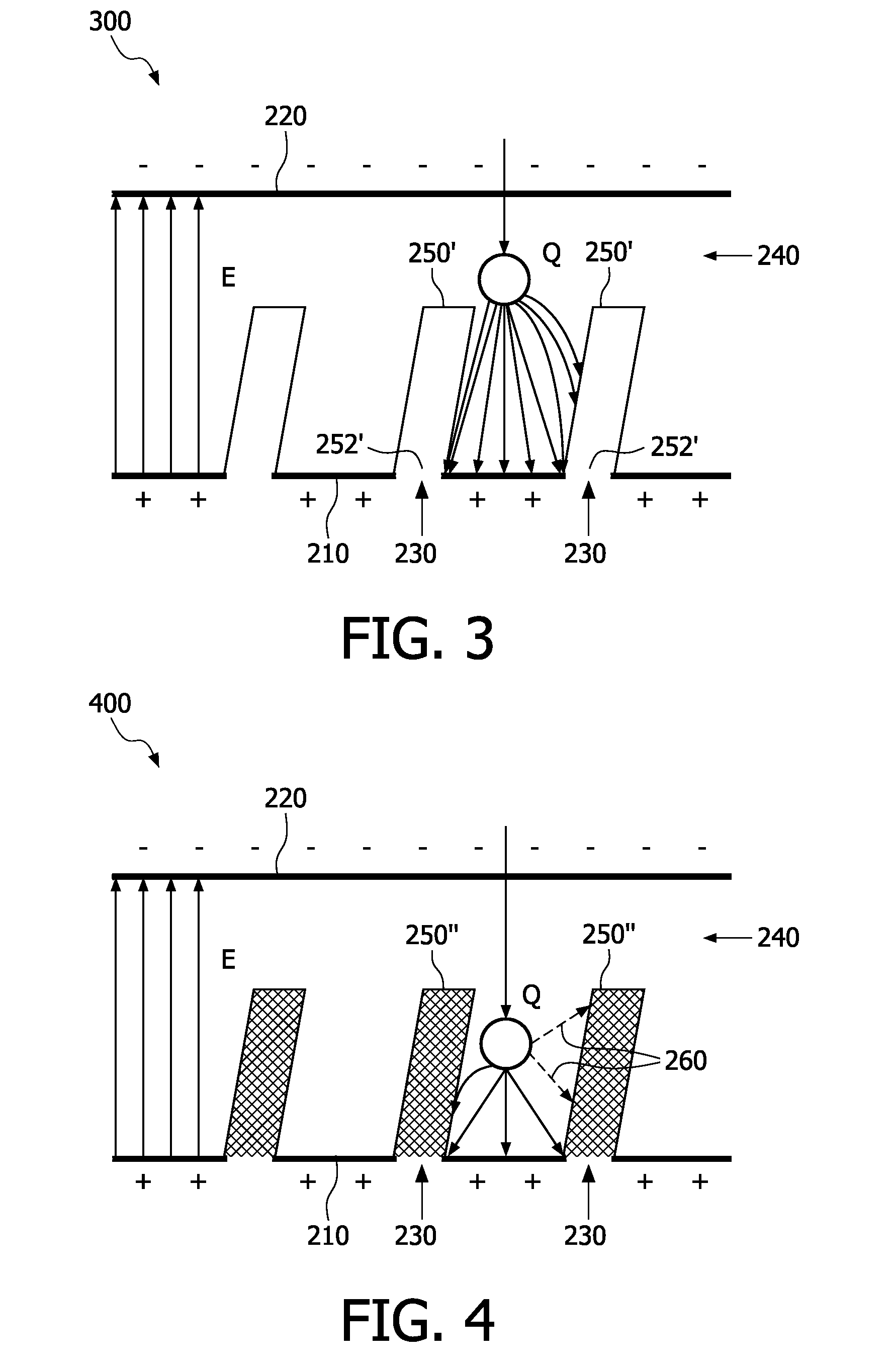
[0018]Another embodiment is shown in FIG. 3, in which the direction of exten...


PUM


Abstract

To mitigate the influence of charge sharing occurring in semiconductor detectors, an improved semiconductor detector (200) is provided, which comprises: a plurality of anodes (210) arranged to form at least one opening (230), each opening being formed by two anodes in the plurality of anodes; at least one cathode (220); a detector cell (240) located between the plurality of anodes and the at least one cathode; wherein the detector cell comprises at least one groove (250), each of the at least one groove having a first opening (252) aligned with one of the at least one opening being formed by two anodes in the plurality of anodes, each of the at least one groove extending towards the at least one cathode. By forming grooves in the detector cell, the charge cloud generated by a single photon can be received by a corresponding anode instead of several neighboring anodes, which thereby improves the spectral resolution and count rate of a semiconductor detector.

Description

FIELD OF THE INVENTION[0001]The present invention relates to a semiconductor detector, particularly to a medical semiconductor detector.BACKGROUND OF THE INVENTION[0002]In medical industry, direct conversion materials, such as Si, GaAs, CdTe, and CZT gain more and more importance in modalities, such as CT detectors, X-ray detectors, Gamma detectors, and nuclear medicine in which the scintillator type detectors are still state of the art. Their advantage over scintillators is the possibility of photon-counting coupled with a good energy solution. However, these direct conversion materials are vulnerable because of charge sharing, a phenomenon in which the charge cloud generated by a single photon is collected by several neighboring electrodes. FIG. 1 shows that a charge cloud generated by one photon is collected by three neighboring electrodes. The phenomenon of charge sharing disturbs the spectral resolution and count rate performance of detectors. In high-rate detectors, the phenom...

Claims


Application Information

Patent Timeline
Patent Type & Authority Patents(United States)
IPC IPC(8): H01L27/146
CPCH01L27/14659H01L27/1463
Inventor ROESSL, EWALDPROKSA, ROLAND
Owner KONINK PHILIPS ELECTRONICS NV
Why Eureka
Try Eureka