Insulated gate bipolar transistor

a bipolar transistor and gate technology, applied in the direction of basic electric elements, electrical equipment, semiconductor devices, etc., can solve the problems of reducing the area of the main cell, increasing production costs, and difficult to discharge holes to the emitter side via the main cell

Active Publication Date: 2013-04-23
SEMICON COMPONENTS IND LLC
View PDF6 Cites 1 Cited by
  • Summary
  • Abstract
  • Description
  • Claims
  • Application Information

AI Technical Summary

Benefits of technology

[0013]The preferred embodiments of the present invention have been developed in view of the above-mentioned and / or other problems in the related art. The preferred embodiments of the present invention can significantly improve upon existing methods and / or apparatuses.
[0014]Among other potential advantages, some embodiments can provide an insulated gate bipolar transistor capable of enhancing hole accumulation effect while controlling decrease in current density.

Problems solved by technology

This in turn increases the production cost due to the thicker epitaxial growth of the drift layer.
However, this structure decreases the area of the main cell, which makes it difficult to discharge holes to the emitter side via the main cell.
The aforementioned conventional technique, however, causes decreased current density due to the decreased area ratio of the main cell.

Method used


Image

  • Insulated gate bipolar transistor
  • Insulated gate bipolar transistor
  • Insulated gate bipolar transistor

Examples


first embodiment

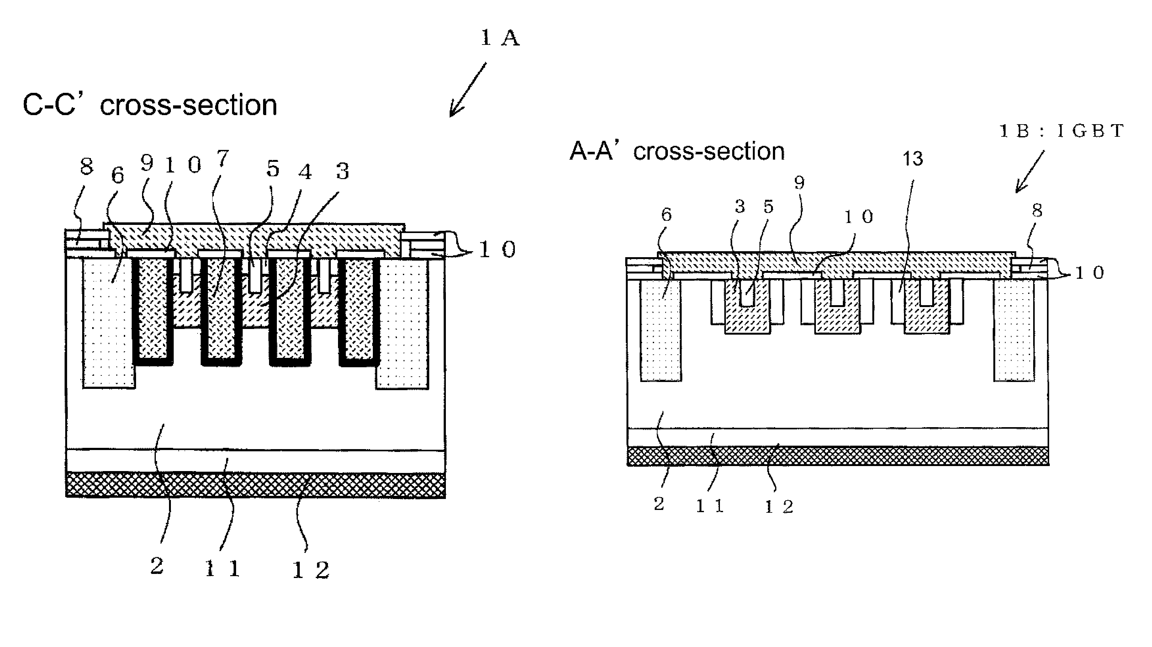
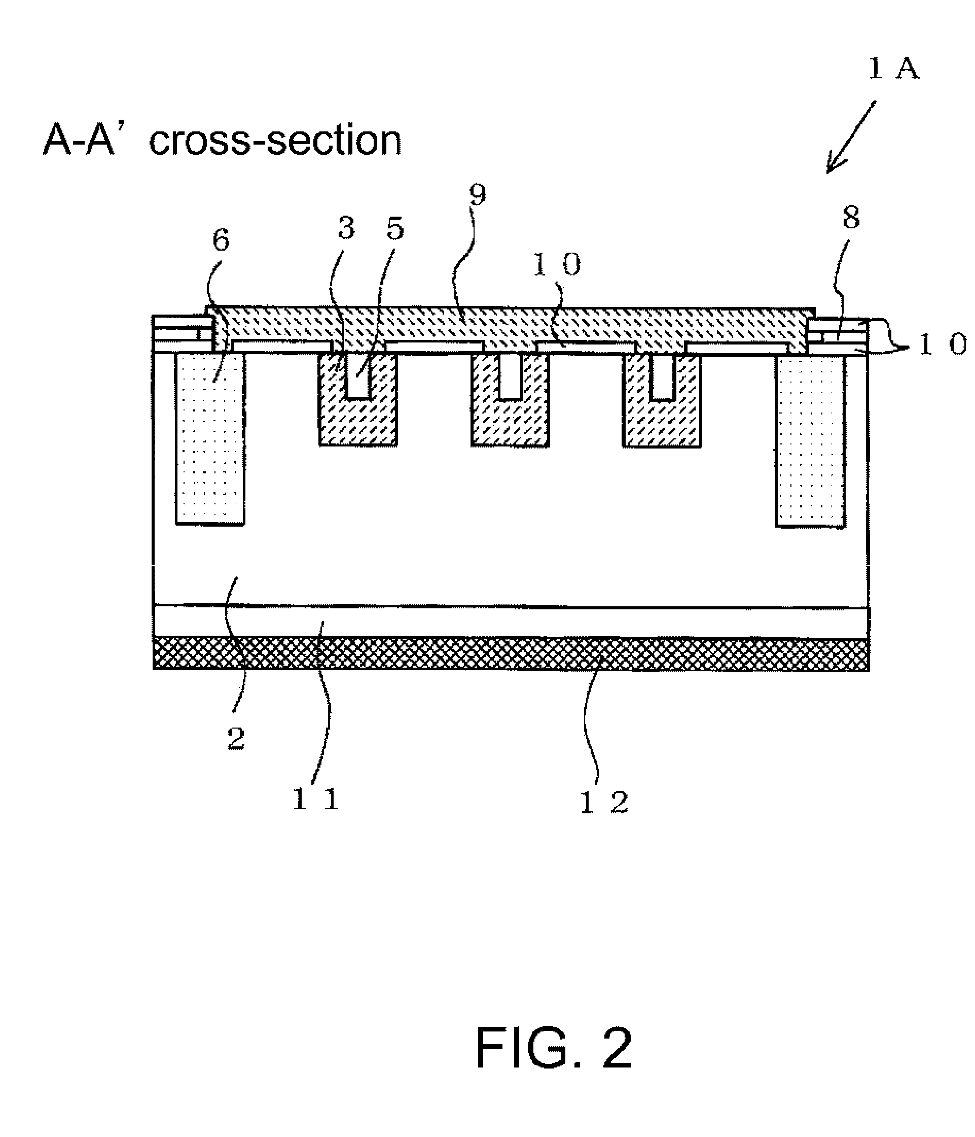
[0043]The structure of an insulated gate bipolar transistor (IGBT) 1A according to a first embodiment of the present invention will be concretely explained with reference to FIGS. 1 to 5. FIGS. 2, 3, 4, and 5 are cross-sectional views taken along the lines A-A′, B-B′, C-C′, and D-D′ in FIG. 1, respectively.

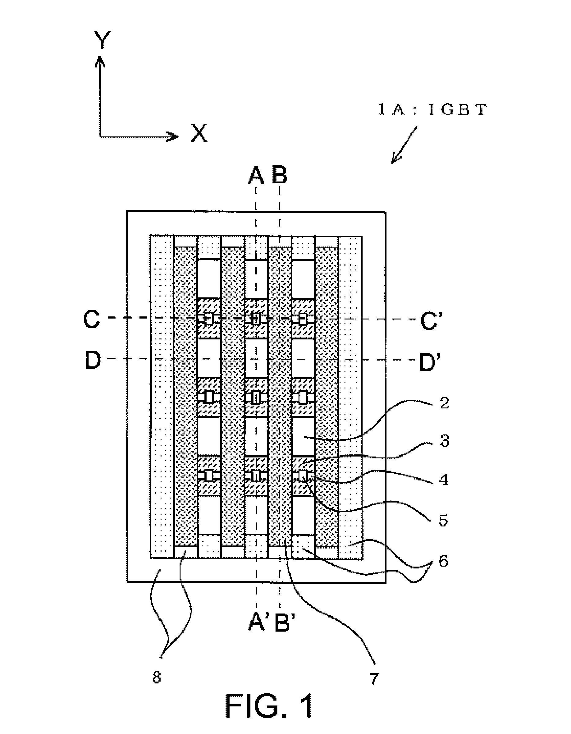
[0044]Referring to FIG. 1, the structure of the insulated gate bipolar transistor (IGBT) according to the first embodiment of the present invention as seen from the top will be explained. This isolated gate bipolar transistor (IGBT) 1A includes a drift layer 2, a base region 3, an emitter region 4, a body region 5, a guard ring 6, a gate electrode 7, and a gate connection line 8. In the actual structure, an emitter electrode 9 connected to the emitter region 4, interlayer insulation films 10 for insulating the emitter electrode 9 from the drift layer 2 or the gate electrode 7 are formed, but these are not illustrated in the plan view for the sake of simplicity.

[0045]Hereinafter, e...

second embodiment

[0069]Next, with referring to FIG. 6, an insulated gate bipolar transistor (IGBT) 1B according to a second embodiment of the present invention will be explained. This insulated gate bipolar transistor (IGBT) 1B has been further enhanced in hole accumulation effect than the aforementioned insulated gate bipolar transistor (IGBT) 1A of the first embodiment.

[0070]FIG. 6 shows a cross-sectional structure of the insulated gate bipolar transistor (IGBT) 1B of this second embodiment which corresponds to the A-A′ cross-section (FIG. 2) of the insulated gate bipolar transistor (IGBT) 1A of the first embodiment.

[0071]Comparing to the first embodiment, in the insulated gate bipolar transistor (IGBT) 1B of this embodiment, an N type conductive type hole discharge control regions 13 are formed on the side surfaces of the base regions 3. Since the other structure is the same as mentioned above, the cumulative explanation will be omitted.

[0072]The function of this structure will be explained. When...

third embodiment

[0073]Next, an insulated gate bipolar transistor (IGBT) 1C of a third embodiment of the present invention will be explained with referring to FIGS. 7 and 8. FIG. 7 is a plan view of the insulated gate bipolar transistor (IGBT) 1C of this embodiment, and FIG. 8 is a cross-sectional view taken along the line E-E′ in FIG. 7.

[0074]In this insulated gate bipolar transistor (IGBT) 1C, the base regions 3 are arranged so as to shift with each other in the region between the adjacent gate electrodes 7. At the portion where the base region 3 is formed in the region between the adjacent gate electrodes 7, a current pathway is formed and holes are discharged. On the other hand, at the portion where the base region is not formed in the region between the adjacent gate electrodes 7, an interlayer insulation film 10 is formed between the emitter electrode 9 and the drift layer 2. Therefore, the discharge of holes is controlled. With this structure, in the insulated gate bipolar transistor (IGBT) 1...


PUM


Abstract

In some embodiments, an insulated gate bipolar transistor includes a drift layer, insulation gates formed at a principle surface portion of the drift layer, base regions formed in a between-gate region, an emitter region formed in the base region so as to be adjacent to the insulation gate, an emitter electrode connected to the emitter region, a collector layer formed at the other side of the principle surface portion of the drift layer, and a collector electrode connected to the collector layer. The conductive type base regions are separated with each other by the drift layers, and the drift layer and the emitter electrode are insulated by an interlayer insulation film.

Description

[0001]This application claims priority under 35 U.S.C. §119 to Japanese Patent Application No. 2009-77063 filed on Mar. 26, 2009, the entire disclosure of which is incorporated herein by reference in its entirety.BACKGROUND OF THE INVENTION[0002]1. Field of the Invention[0003]The present invention relates to an insulated gate bipolar transistor (IGBT) for use as, e.g., a switching element in the field of power electronics.[0004]2. Description of the Related Art[0005]The following description sets forth the inventor's knowledge of related art and problems therein and should not be construed as an admission of knowledge in the prior art.[0006]An insulated gate bipolar transistor (IGBT) is noted for high efficiency and fast switching, and used as a switching element in the field of power electronics.[0007]The insulated gate bipolar transistor (IGBT) is classified into a PT (punch-through) structure and a NPT (non punch-through) structure. The punch-through structure includes a collecto...

Claims


Application Information

Patent Timeline
Patent Type & Authority Patents(United States)
IPC IPC(8): H01L29/66
CPCH01L29/0619H01L29/0696H01L29/7397
Inventor YONEDA, SHUJISAWAMURA, KENJI
Owner SEMICON COMPONENTS IND LLC
Why Eureka
Try Eureka