
Multi-port memory device with serial input/output interface

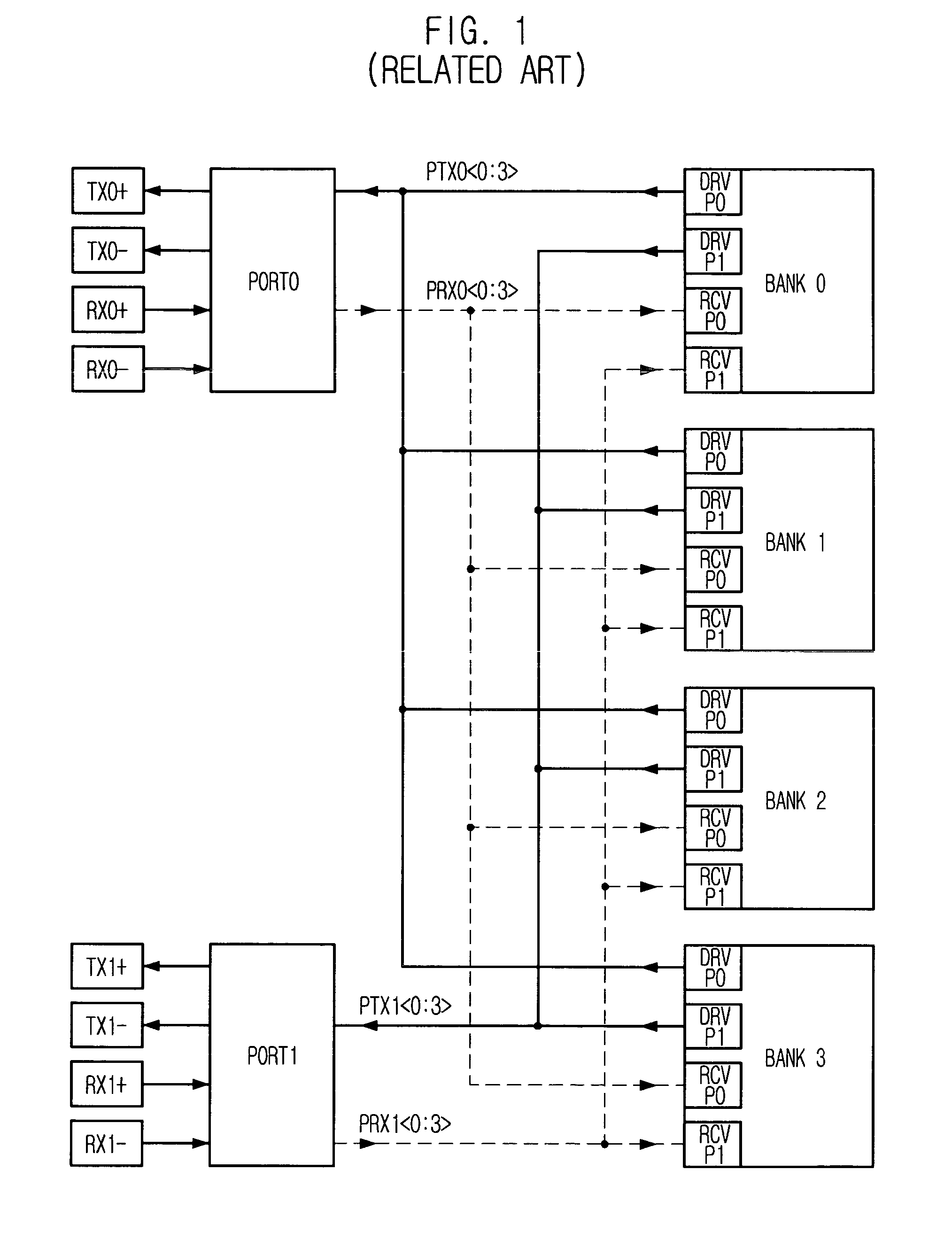
a memory device and serial input technology, applied in the field of multi-port memory devices, can solve the problems of increasing manufacturing costs and difficulty in determining whether the fault occurs in the port or in the bank

Active Publication Date: 2013-04-23
SK HYNIX INC
View PDF27 Cites 5 Cited by
  • Summary
  • Abstract
  • Description
  • Claims
  • Application Information

AI Technical Summary

Benefits of technology

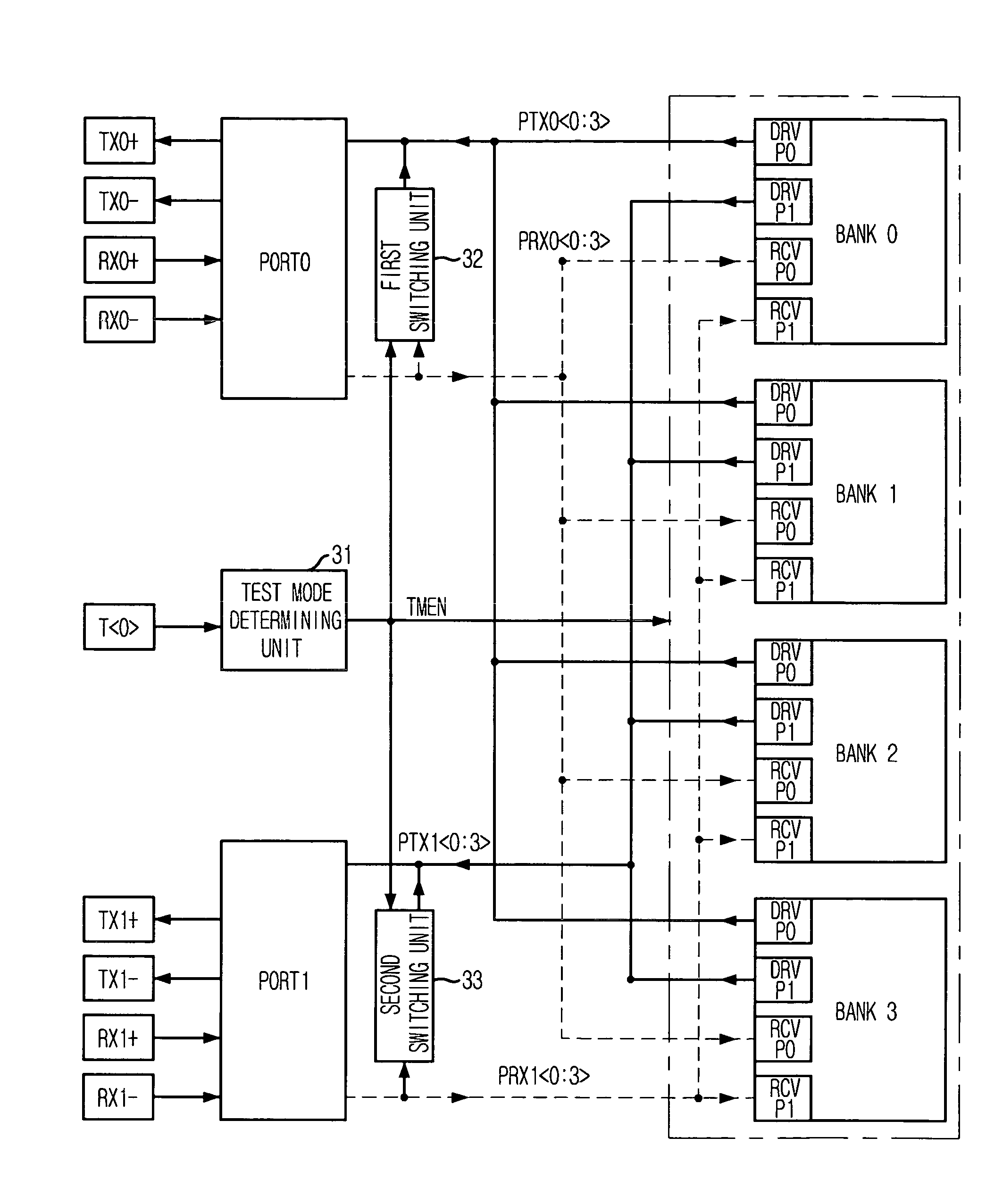
The present invention provides a multi-port memory device capable of detecting faults of ports converting parallel / serial data regardless of faults of banks having a core. The device includes a plurality of serial input / output data pads, ports, banks, data buses, and a switching unit for connecting the data buses. Additionally, the invention includes a test mode determination unit for generating a test mode enable signal in response to a mode control signal, and a plurality of switching units for connecting the data buses in response to the test mode enable signal. This allows for efficient testing of the ports and banks in a multi-port memory device.

Problems solved by technology

Consequently, as distance increases, the manufacturing cost increases.
Accordingly, it is difficult to determine whether the faults occur in the ports or in the bank having the DRAM core.

Method used


Image

  • Multi-port memory device with serial input/output interface
  • Multi-port memory device with serial input/output interface
  • Multi-port memory device with serial input/output interface

Examples


Embodiment Construction

[0041]Hereinafter, a multi-port memory device with a serial input / output (I / O) interface in accordance with exemplary embodiments of the present invention will be described in detail with reference to the accompanying drawings.

[0042]FIG. 3 is a block diagram of a multi-port memory device in accordance with an embodiment of the present invention. For convenience of explanation, the multi-port memory device having two ports and four banks is illustrated.

[0043]The multi-port memory device includes a plurality of serial I / O pads TX0+, TX0−, TX1+, TX1−, RX0+, RX0−, RX1+ and RX1−, a test mode control pad T0>, a test mode determination unit 31, first and second switching units 32 and 33, first and second ports PORT0 and PORT1, first to fourth banks BANK0 to BANK3, and a plurality of global input / output (I / O) data buses PTX00:3>, PTX10:3>, PRX00:3>, and PRX10:3>.

[0044]The plurality of serial I / O pads support a data communication between the port PORT0 and the second port PORT1 and external ...


PUM


Abstract

A multi-port memory device includes a plurality of serial I / O data pads for providing a serial input / output (I / O) data communication; a plurality of ports for performing the serial I / O data communication with external devices through the serial I / O data pads; a plurality of banks for performing a parallel I / O data communication with the ports; a plurality of first data buses for transferring first signals from the ports to the banks; a plurality of second data buses for transferring second signals from the banks to the ports; and a switching unit for connecting the first data buses with the second data buses in response to a control signal.

Description

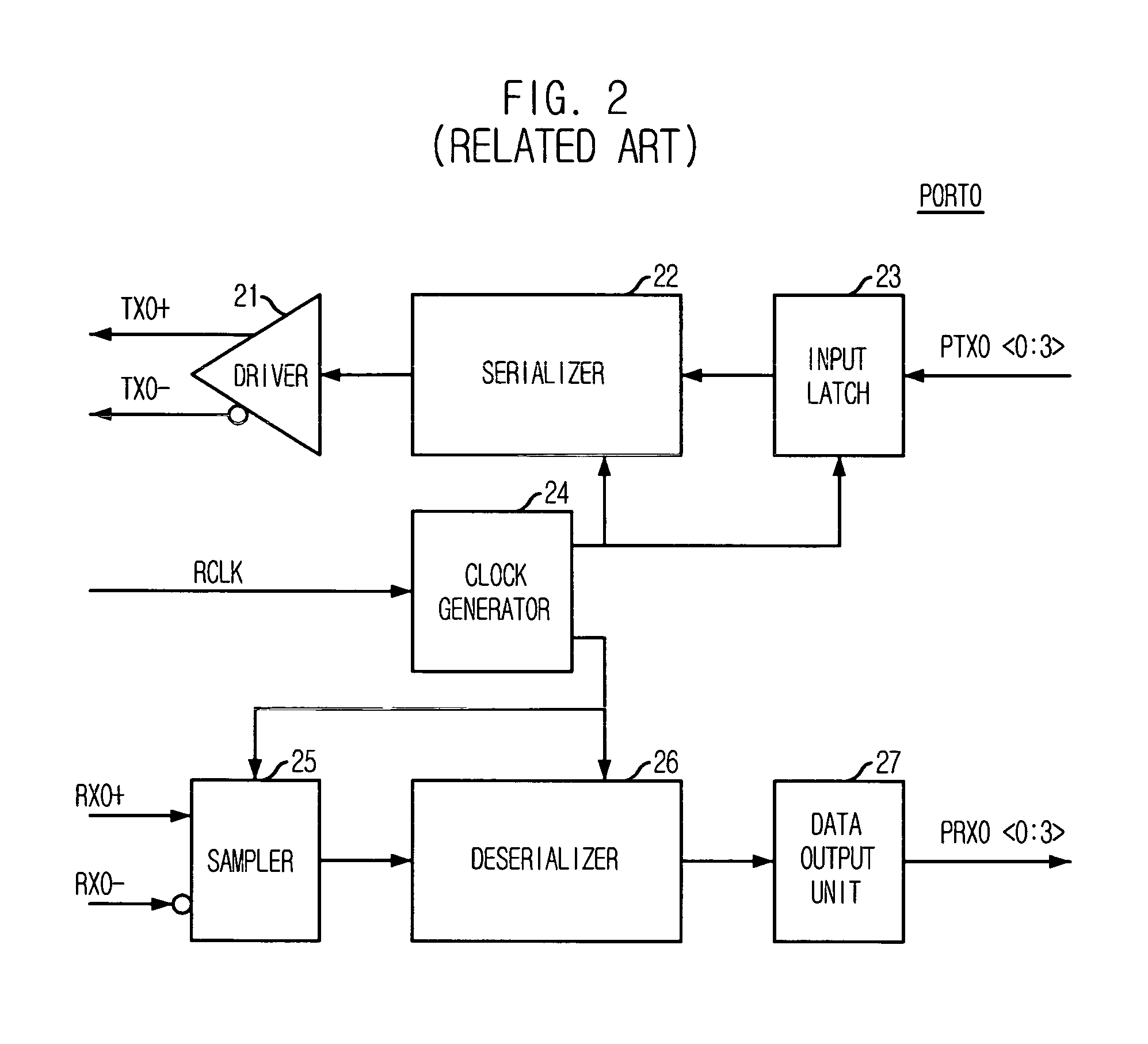
FIELD OF THE INVENTION[0001]The present invention relates to a multi-port memory device; and, more particularly, to a multi-port memory device with a serial input / output (I / O) interface for detecting faults of ports converting parallel / serial data regardless of faults of banks having a core.DESCRIPTION OF RELATED ARTS[0002]Generally, most memory devices including random access memory (RAM) have a single port with a plurality of input / output pin sets. That is, the single port is provided for data exchange between a memory device and an external chipset. Such a memory device having the single port uses a parallel input / output (I / O) interface to simultaneously transmit multi-bit data through signal lines connected to a plurality of input / output (I / O) pins. The memory device exchanges data with the external device through a plurality of I / O pins in parallel.[0003]The I / O interface is an electrical and mechanical scheme to connect unit devices having different functions through signal li...

Claims


Application Information

Patent Timeline
Patent Type & Authority Patents(United States)
IPC IPC(8): G06F13/38
CPCG11C7/1006G11C7/1075G11C7/22G11C8/16G11C29/02G11C29/022G11C2207/107
Inventor DO, CHANG-HO
Owner SK HYNIX INC
Learn More