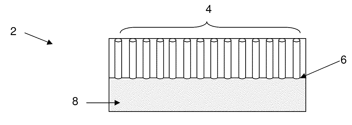
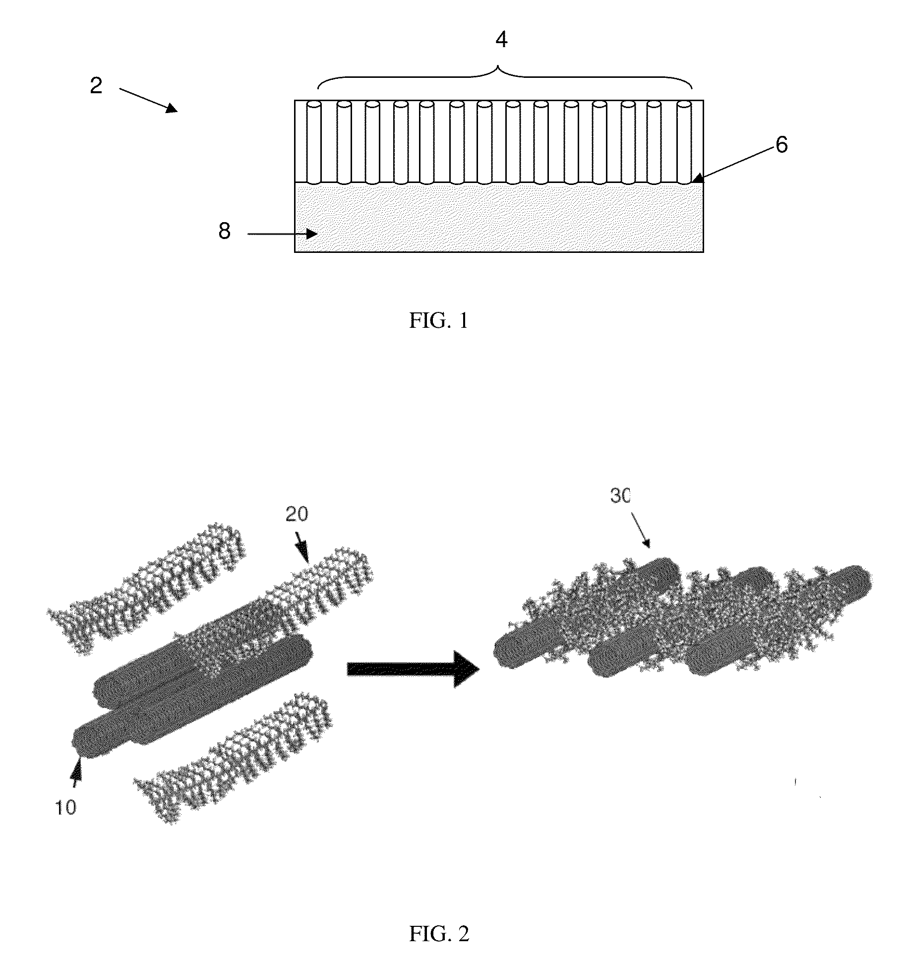
Field emission devices including nanotubes or other nanoscale articles
a field emission device and carbon nanotube technology, applied in the direction of discharge tube luminescnet screen, fluorescence/phosphorescence, instruments, etc., can solve the problems of high cost of fabrication, limited current technology, and field emission
- Summary
- Abstract
- Description
- Claims
- Application Information
AI Technical Summary
Problems solved by technology
Method used
Image

Examples
example 1
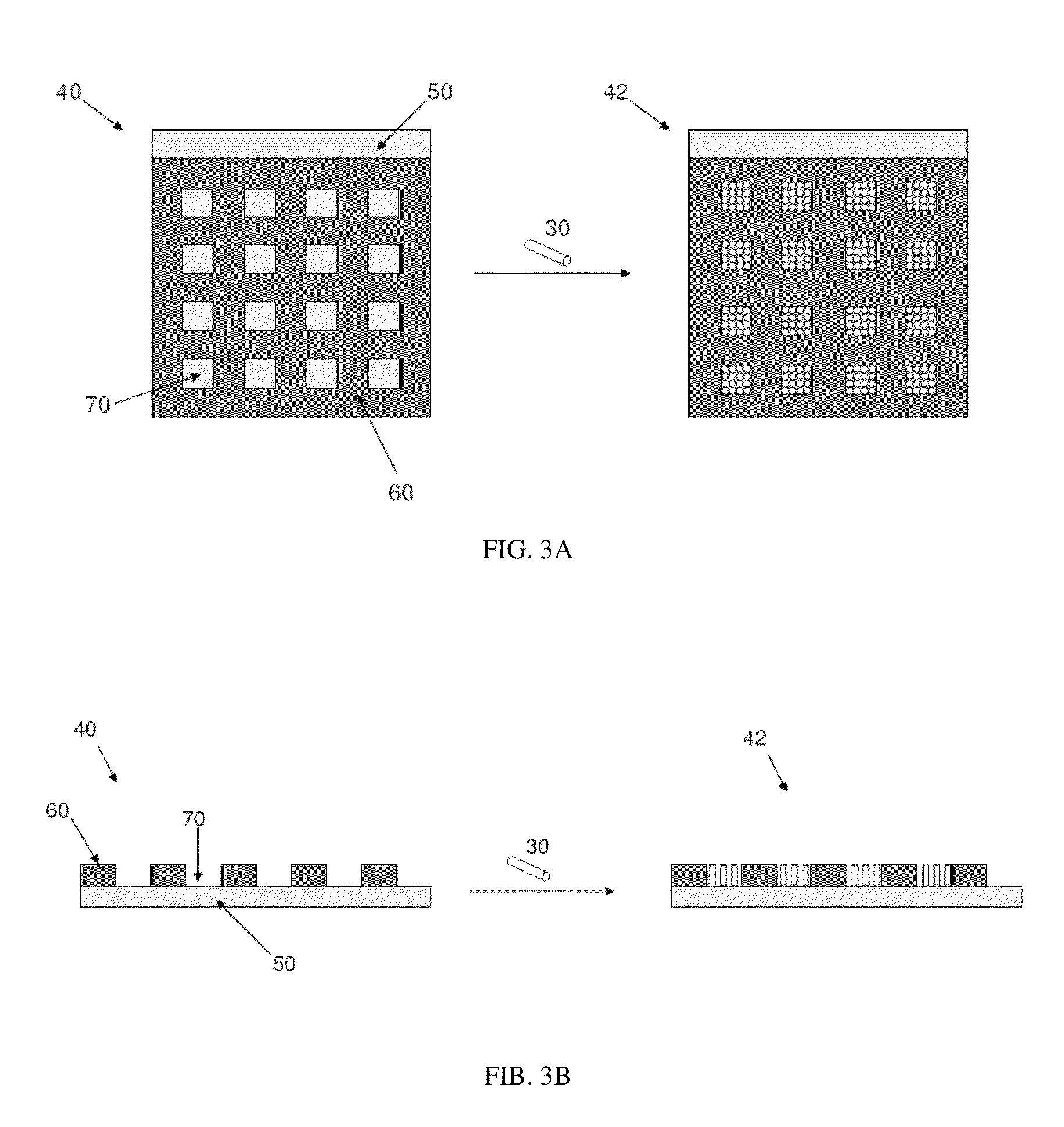
[0057]Single-walled carbon nanotubes were purchased from Carbon Nanotechnologies Inc. (CNI Lot #R0204). The carbon nanotubes were combined with high molecular weight poly(3-hexylthiophene), a polymeric surfactant, to form a stable carbon nanotube suspension. Next, an anode and a cathode (e.g., a gold cathode), spaced 1-2 mm apart, were immersed within the suspension, as shown by the photograph in FIG. 5A. Using an Autolab electrochemical station, a DC bias voltage (5 V) was applied to the suspension and substrate for nanotube deposition, with the cathode serving as the substrate. The deposition speed was 4 microns / second.
[0058]The absorption spectrum of the assembly of carbon nanotubes was measured between two ITO slides. FIG. 6A shows the UV-visible absorption spectra of the assembly of carbon nanotubes after (a) 0 minutes, (b) 1 minute, (c) 10 minutes, and (d) 20 minutes of electrophoretic deposition on the substrate. FIG. 6B shows the near-IR absorption spectra of an assembly of ...
example 2
[0060]The resistance of a carbon nanotube assembly formed by electrophoretic deposition as described herein was compared to the resistance of a carbon nanotube assembly formed by spin-coating. The electrophoretically deposited assembly had a resistance of 30 Ohms, while the spin-coated assembly exhibited a resistance of approximately 3000 Ohms. Thus, the resistance of the electrophoretically deposited assembly comprising a high degree of aligned carbon nanotubes was 100 times greater than the spin-coated assembly comprising a relatively lower degree of aligned carbon nanotubes.
PUM
| Property | Measurement | Unit |
|---|---|---|
| voltage | aaaaa | aaaaa |
| surface area | aaaaa | aaaaa |
| surface area | aaaaa | aaaaa |
Abstract
Description
Claims
Application Information