Method of fabricating sub-100 nanometer field emitter tips comprising group III-nitride semiconductors

a semiconductor and sub-100 nanometer field technology, applied in the manufacture of electrode systems, electric discharge tubes/lamps, electric discharge tubes, etc., can solve the problem of more geometrically complex devices being fabricated more easily, and achieve the effect of fast, robust and cost effective technique, prolonging device life, and reducing manufacturing costs

Inactive Publication Date: 2005-11-01
UNITED STATES OF AMERICA THE AS REPRESENTED BY THE SEC OF THE ARMY
View PDF9 Cites 44 Cited by
  • Summary
  • Abstract
  • Description
  • Claims
  • Application Information

AI Technical Summary

Benefits of technology

[0014]Other advantages of the invention are that it solves several problems, which currently plague the field emitter production industry, and provides the industry with a fast, robust, and cost effective technique for producing gallium nitride or other group III-nitride semiconductor field emitters (such as aluminum nitride field emitters). For example, through its unique methodology in fabrication of the field emitters, vacuum microelectronic devices with the capability of vacuum tubes will be available with the added benefit of faster turn-on because field emitters do not have to be warmed up as vacuum tubes do. Furthermore, the invention achieves device miniaturization and extends the device lifetime due to the materials used in the fabrication of the emitter tips as well as the

Problems solved by technology

Furthermore, more geometrically complex

Method used


Image

  • Method of fabricating sub-100 nanometer field emitter tips comprising group III-nitride semiconductors
  • Method of fabricating sub-100 nanometer field emitter tips comprising group III-nitride semiconductors
  • Method of fabricating sub-100 nanometer field emitter tips comprising group III-nitride semiconductors

Examples


Embodiment Construction

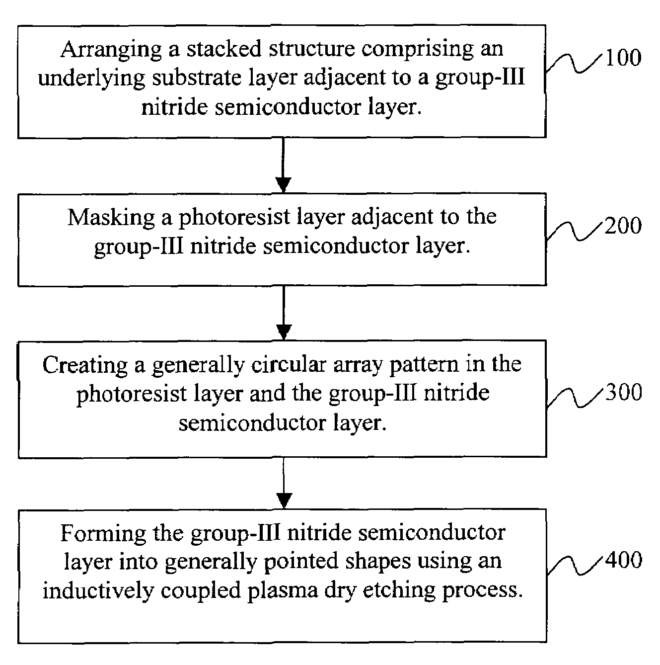
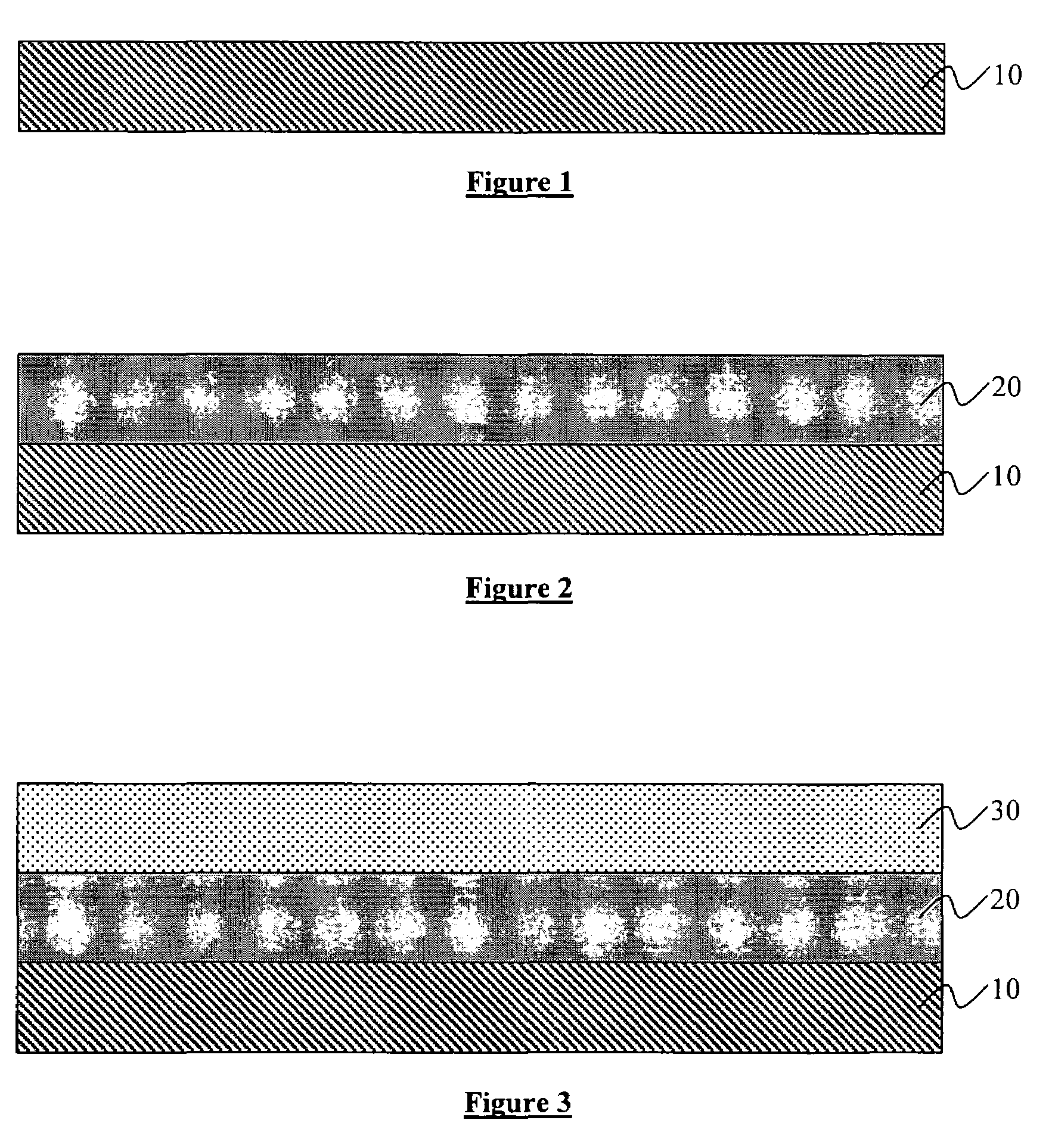
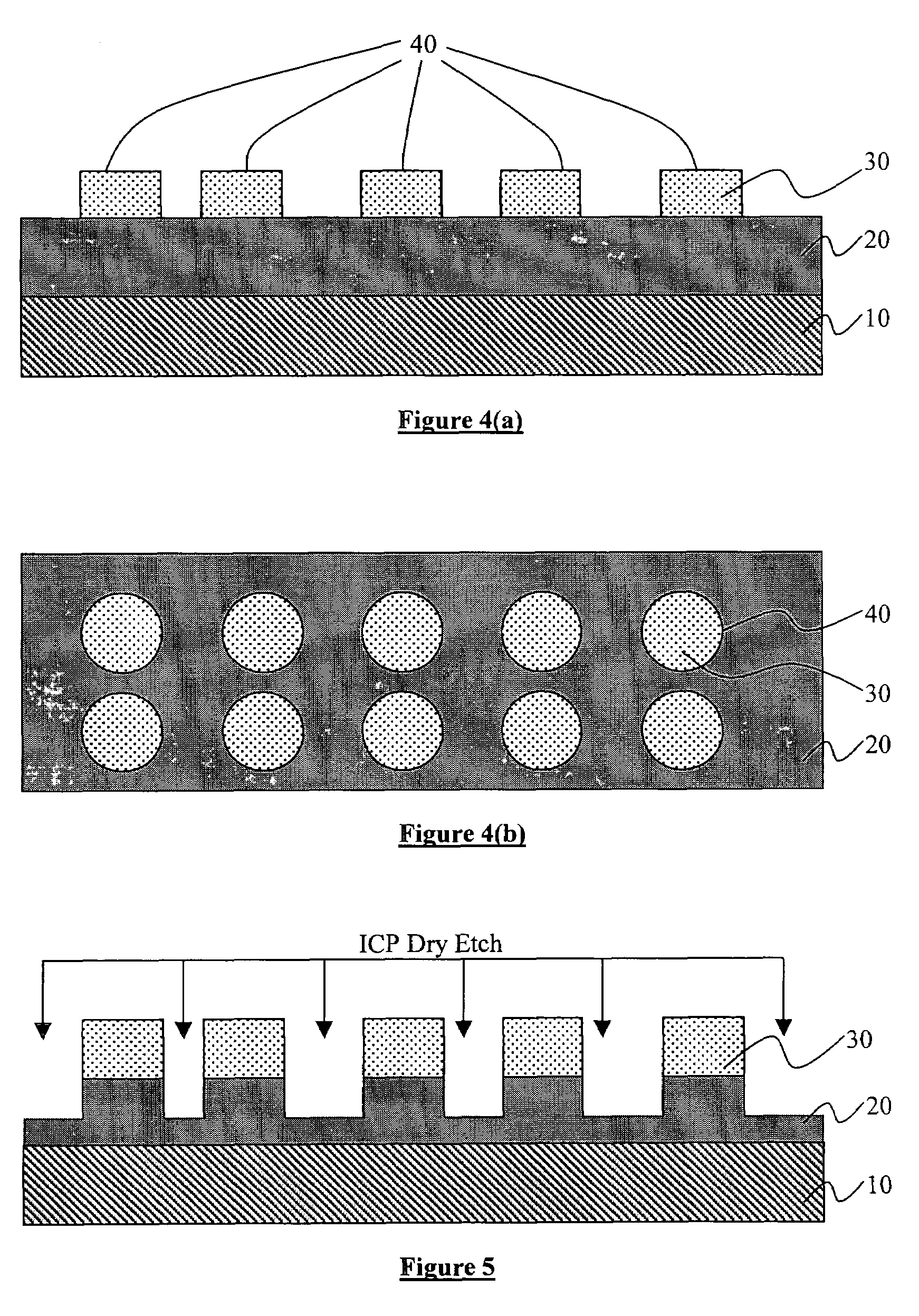
[0026]As previously mentioned, there is a need for an improved process of fabricating a sub-100 nanometer field emitter tip out of group III-nitride semiconductors for use in vacuum microelectronic devices, which overcome the deficiencies of the conventional approaches and results in higher quality field emitter tips. Referring now to the drawings, and more particularly to FIGS. 1 through 8, there are shown preferred embodiments of the invention.

[0027]An embodiment of the invention provides an improvement to conventional field emitter fabrication techniques. The invention is a cost effective technique for producing field emitter tips made of group III-nitride semiconductors such as gallium nitride by using a dry etching (reactive ion etching) technique such as an inductive coupled plasma etching technique rather than a conventional growth or material deposition technique. These tips have a radius of curvature of less than 100 nm for use in vacuum microelectronic devices. The procedu...


PUM


Abstract

A method of producing a field emission device includes laying a group III-nitride semiconductor layer over a substrate, placing a photoresist mask over the group III-nitride semiconductor layer, patterning a generally circular grid in the photoresist mask and the group III-nitride semiconductor layer, and forming the group III-nitride semiconductor layer into generally pointed tips using an inductively coupled plasma dry etching process, wherein the group III-nitride semiconductor layer comprises a group III-nitride semiconductor material having a low positive electron affinity or a even a negative electron affinity, wherein the inductively coupled plasma dry etching process selectively creates an anisotropic deep etch in the group III-nitride semiconductor layer, and wherein the inductively coupled plasma dry etching process creates an isotropic etch in the group III-nitride semiconductor layer. Preferably, the photoresist layer is approximately 1.7 microns in thickness, and the fabricated tips have a radius of curvature of less than 100 nanometers.

Description

GOVERNMENT INTEREST[0001]The invention described herein may be manufactured, used, and / or licensed by or for the United States Government.BACKGROUND OF THE INVENTION[0002]1. Field of the Invention[0003]The present invention generally relates to methods of manufacturing field emitters, and more particularly to a method of fabricating a sub-100 nanometer field emitter tip out of group III-nitride semiconductors for use in vacuum microelectronic devices.[0004]2. Description of the Related Art[0005]The quantum-mechanical phenomenon known as field emission, otherwise referred to as cold emission, occurs when electrons tunnel through an energy barrier at an emitter surface / vacuum interface and through a vacuum subjected to an applied electric field. Typically, the emitter surface is a metal or semiconductor material. This field emission of electrons provides a cold cathode for use in flat panel displays and other vacuum microelectronic devices and applications.[0006]The electron affinity ...

Claims


Application Information

Patent Timeline
IPC IPC(8): H01L21/02H01L21/302H01J9/02
CPCH01J9/025H01J2237/3341
Inventor SHAH, PANKAJ B.
Owner UNITED STATES OF AMERICA THE AS REPRESENTED BY THE SEC OF THE ARMY
Why Eureka
Try Eureka