Method for manufacturing carbon nanotube field emission device

a carbon nanotube and field emission technology, applied in the manufacture of electric discharge tubes/lamps, mechanical vibration separation, discharge tubes luminescnet screens, etc., can solve the problems of poor electrical contact between carbon nanotubes and substrates, high emission voltages to emit electrons, and inability to reliably carry high electric currents. to achieve the effect of avoiding the separation of carbon nanotubes

Active Publication Date: 2008-11-11
HON HAI PRECISION IND CO LTD +1
View PDF11 Cites 44 Cited by
  • Summary
  • Abstract
  • Description
  • Claims
  • Application Information

AI Technical Summary

Benefits of technology

[0007]The present invention provides a carbon nanotube field emission device including a substrate and a carbon nanotube array formed on and secured to the substrate. In a preferred embodiment, an adhesive is applied to secure the carbon nanotubes on the substrate. This avoids separation of the carbon nanotubes from the substrate by electric field force in a strong electric field. Tips of the carbon nanotubes are exposed.
[0013]Compared with a conventional carbon nanotube field emission device, the carbon nanotube field emission device of the preferred embodiment has the following advantages. Firstly, the carbon nanotubes are secured on the substrate by the adhesive. This avoids the carbon nanotubes being pulled out from the substrate by electric field force in a strong electric field. Secondly, the surface of the carbon nanotube array is treated by laser, thus the adhesive at the surface is removed, and the tips of the carbon nanotubes are exposed. This helps ensure that the carbon nanotube field emission device has reduced shielding between adjacent carbon nanotubes, reduced threshold voltage, and increased field emission current. Further, the carbon nanotube field emission device can emit electrons uniformly and stably.

Problems solved by technology

However, such materials need high emission voltages to emit electrons, and cannot carry high electric currents reliably.
Secondly, the mixture is printed on the substrate.
Therefore, the electrical contact between the carbon nanotubes and the substrate is bad.
The typical result of such bad contact is that the carbon nanotube field emission device cannot emit electrons uniformly and stably.
However, the carbon nanotubes are not secured on the substrate.

Method used


Image

  • Method for manufacturing carbon nanotube field emission device
  • Method for manufacturing carbon nanotube field emission device
  • Method for manufacturing carbon nanotube field emission device

Examples


Embodiment Construction

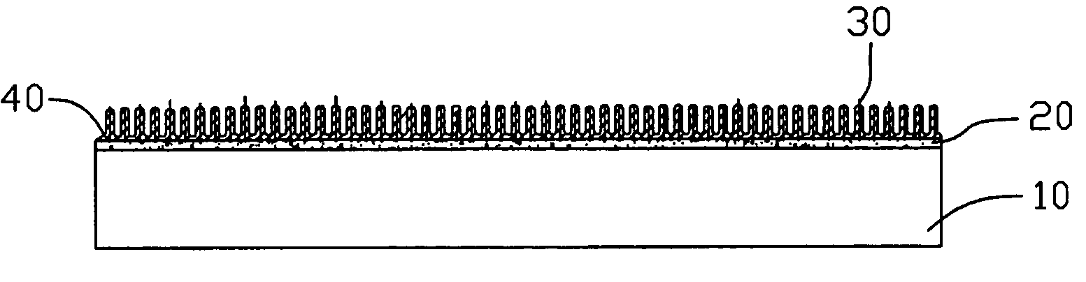
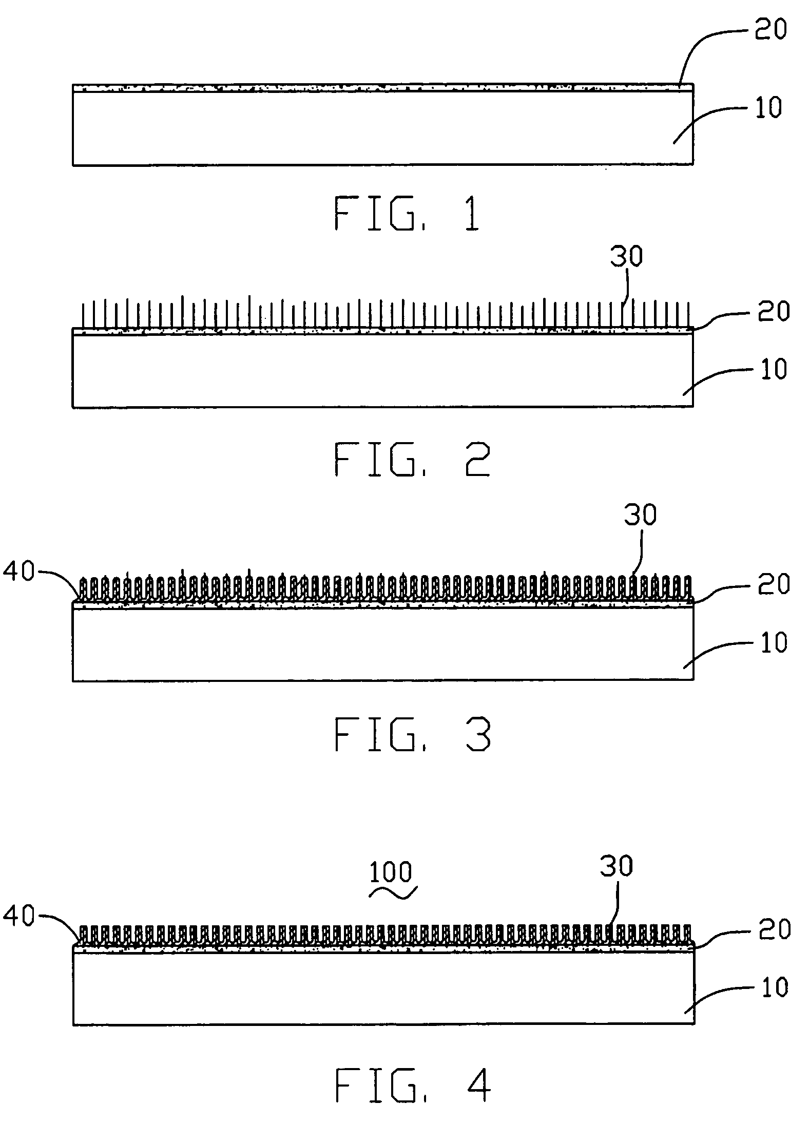
[0021]Referring to FIG. 4, a carbon nanotube field emission device 100 of a preferred embodiment of the present invention is shown. The carbon nanotube field emission device 100 includes a substrate 10, a catalyst film 20 deposited on the substrate 10, and a carbon nanotube array 30 formed on the substrate 10. The carbon nanotube field emission device 100 further adopts an adhesive 40 to secure the carbon nanotube array 30 on the substrate 10. The carbon nanotubes are parallel to each other, and tips of the carbon nanotubes are exposed.

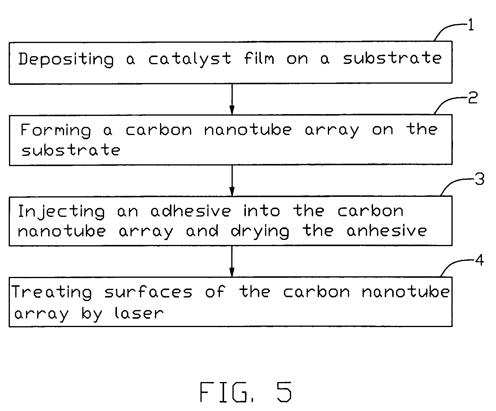
[0022]Referring to FIG. 5, a method for manufacturing the carbon nanotube field emission device 100 includes the steps of:[0023](1) depositing the catalyst film 20 on the substrate 10;[0024](2) forming the carbon nanotube array 30 on the substrate 10;[0025](3) injecting the adhesive 10 into the carbon nanotube array 30, and drying the adhesive 40; and[0026](4) treating surfaces of the carbon nanotube array 30 by laser.

[0027]Referring to FIGS. 1, 2 and...


PUM

PropertyMeasurementUnit
wavelengthaaaaaaaaaa
emission voltagesaaaaaaaaaa
thicknessaaaaaaaaaa

Abstract

A carbon nanotube field emission device (100) includes a substrate (10), and a carbon nanotube array (30) formed on and secured to the substrate. This avoids separation of the carbon nanotubes from the substrate by electric field force in a strong electric field. Tips of the carbon nanotubes are exposed. A method for manufacturing the carbon nanotube field emission device includes the steps of: (a) depositing a catalyst film (20) on a substrate; (b) forming a carbon nanotube array on the substrate; (c) injecting an adhesive into the carbon nanotube array, and drying the adhesive; and (d) treating surfaces of the carbon nanotube array by laser. The carbon nanotube field emission device has reduced shielding between adjacent carbon nanotubes, reduced threshold voltage, and increased field emission current.

Description

BACKGROUND OF THE INVENTION[0001]The invention relates generally to field emission devices and manufacturing methods thereof; and more particularly to a carbon nanotube field emission device and a manufacturing method thereof.[0002]Field emission materials are used in a variety of applications such as, for example, flat panel displays to emit electrons. Typical field emission materials are metals such as, for example, molybdenum (Mo), tantalum (Ta), silicon (Si), and diamond (C). However, such materials need high emission voltages to emit electrons, and cannot carry high electric currents reliably. Carbon nanotubes typically have superior performance; in particular, good electron emission capability at low emission voltages, generally less than 100 volts. Furthermore, carbon nanotubes can carry high electric currents reliably. Due to these properties, carbon nanotubes are considered to be an ideal field emission material for application in a variety of display devices, including fla...

Claims


Application Information

Patent Timeline
Patent Type & Authority Patents(United States)
IPC IPC(8): H01J1/02B05D1/18D01F9/12H01J1/304H01J9/02
CPCB82Y10/00H01J1/304H01J9/025H01J2201/30469
Inventor LIU, YU-MINGLIU, LIANGFAN, SHOU-SHAN
Owner HON HAI PRECISION IND CO LTD
Why Eureka
Try Eureka