Needle fixture of a probe card in semiconductor inspection equipment and needle fixing method thereof

a technology of semiconductor inspection equipment and needle fixture, which is applied in the direction of semiconductor/solid-state device testing/measurement, measurement devices, instruments, etc., can solve the problems of increasing production costs, affecting the reliability of chip testing, and the needle fixture to separate from the probe needle, so as to prevent the cracking improve the performance and inhibit the separation of the adhesion unit

Inactive Publication Date: 2005-05-31
SAMSUNG ELECTRONICS CO LTD
View PDF6 Cites 127 Cited by
  • Summary
  • Abstract
  • Description
  • Claims
  • Application Information

AI Technical Summary

Benefits of technology

[0008]To overcome the above-described problems, it is a first feature of an embodiment of the present invention to provide a needle fixture of a probe card of semiconductor inspection equipment that improves the performance of an adhesion unit for affixing a probe needle to a needle fixture, to prevent a crack of the adhesion unit, or to inhibit separation of the adhesion unit from the needle fixture. It is a second feature of an embodiment of the present invention to provide a needle fixing method in a probe card of semiconductor inspection equipment fixing a probe needle to a needle fixture using an adhesive.

Problems solved by technology

Therefore, due to the temperature variation, the adhesion unit repeatedly contracts and expands, thereby generating a crack in the adhesion unit and thereby causing the probe needle to separate from the needle fixture.
As a result, the reliability of the chip test is diminished.
Moreover, changing a probe card after the adhesion unit becomes cracked or the probe needle has separated from the needle fixture increases production costs.

Method used


Image

  • Needle fixture of a probe card in semiconductor inspection equipment and needle fixing method thereof
  • Needle fixture of a probe card in semiconductor inspection equipment and needle fixing method thereof
  • Needle fixture of a probe card in semiconductor inspection equipment and needle fixing method thereof

Examples


Embodiment Construction

[0021]Korean Patent Application No. 2002-39039, filed Jul. 5, 2002, and entitled: “Needle Fixture of a Probe Card in Semiconductor Inspection Equipment and Needle Fixing Method Thereof,” is incorporated by reference herein in its entirety.

[0022]The present invention will now be described more fully hereinafter with reference to the accompanying drawings, in which preferred embodiments of the invention are shown. The invention may, however, be embodied in different forms and should not be construed as limited to the embodiments set forth herein. Rather, these embodiments are provided so that this disclosure will be thorough and complete, and will fully convey the scope of the invention to those skilled in the art.

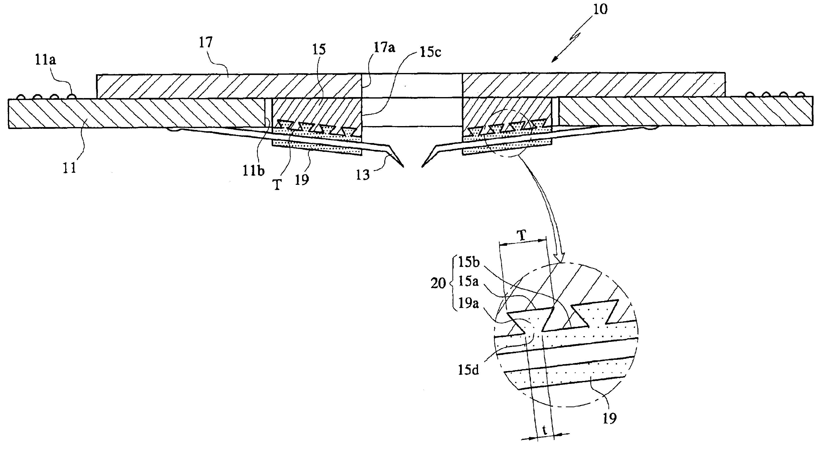
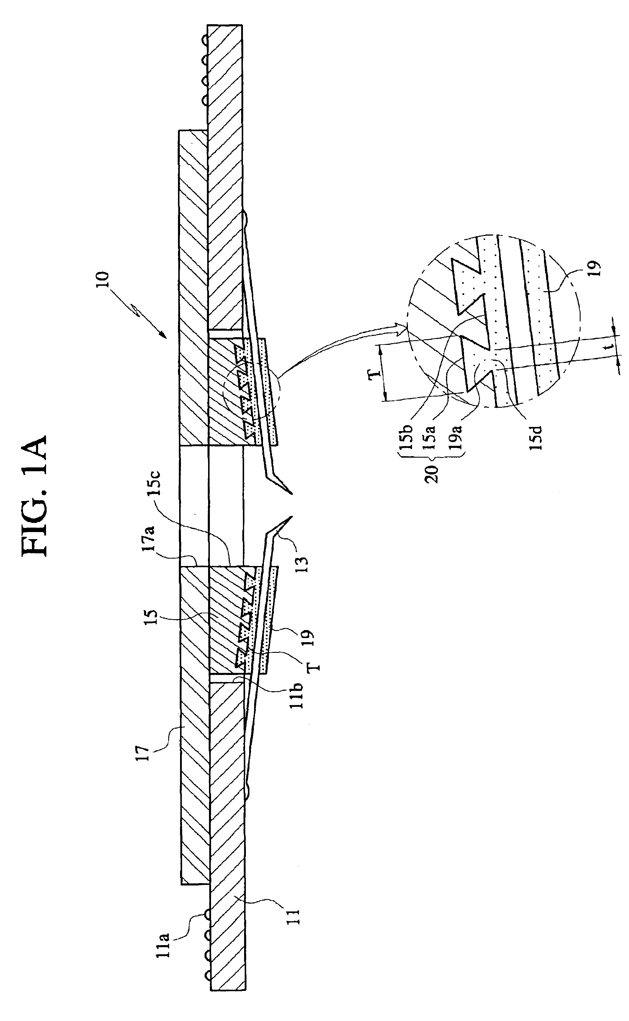
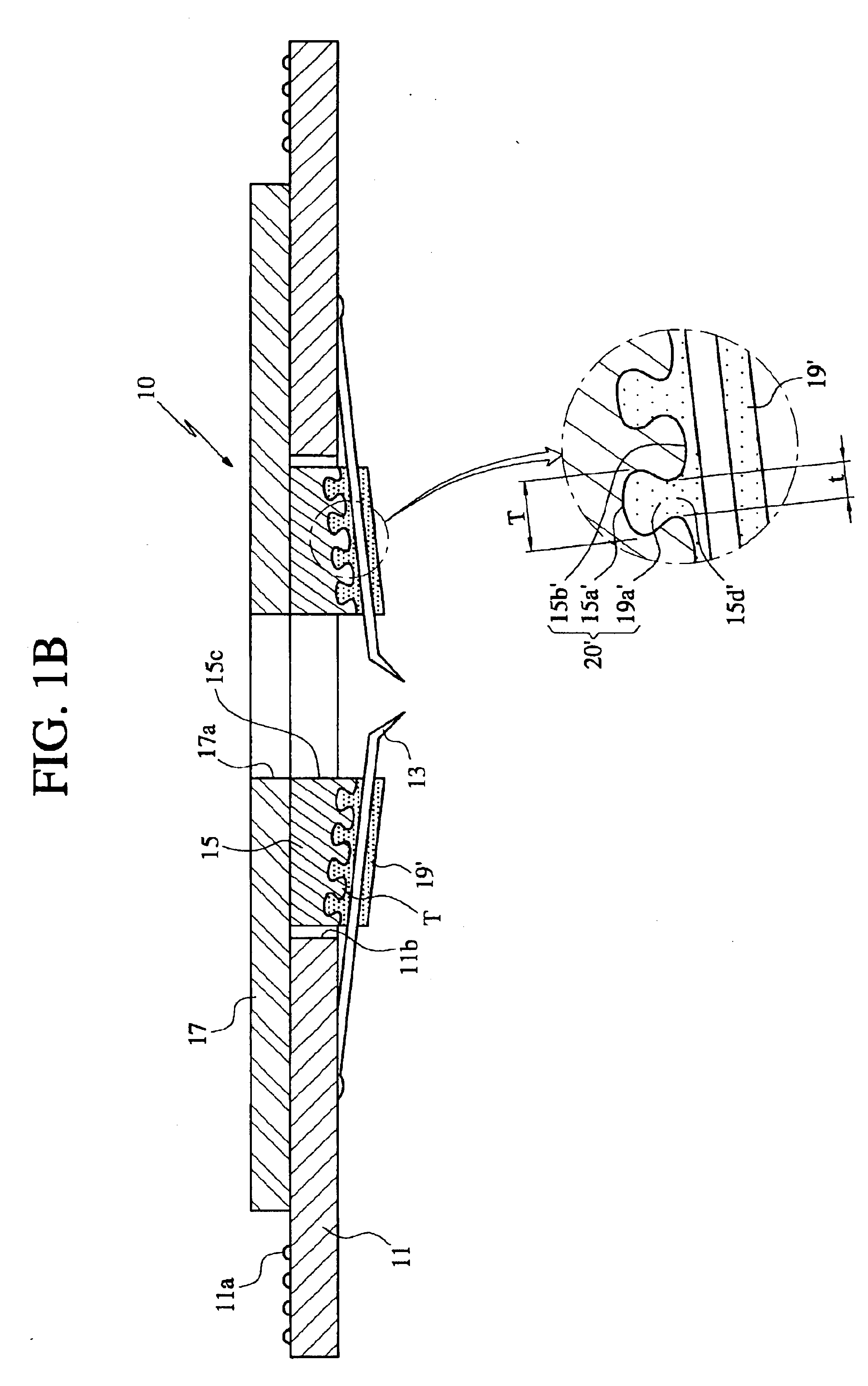
[0023]FIG. 1A illustrates a probe card 10 according to a preferred embodiment of the present invention. FIG. 1B illustrates a probe card 10 according to an alternate embodiment of the present invention. FIG. 2 illustrates a plan view of a bottom of a needle fixture of FIG. 1...


PUM


Abstract

A needle fixture of a probe card and a needle fixing method in semiconductor inspection equipment include a needle fixture of a probe card in semiconductor inspection equipment including a printed circuit board; a needle fixture installed in the printed circuit board; a resin unit affixing a probe needle to the needle fixture using an adhesive; and a separation preventer for preventing separation of the resin unit from the needle fixture, wherein the separation preventer includes: a plurality of notches formed along a bottom surface of the needle fixture; and the adhesive filling the plurality of notches.

Description

BACKGROUND OF THE INVENTION[0001]1. Field of the Invention[0002]The present invention relates to a probe card of semiconductor inspection equipment. More particularly, the present invention relates to a needle fixture of the probe card and a needle fixing method to the probe card using an adhesive wherein the configuration of the needle fixture is changed to strengthen the attachment of the probe needle.[0003]2. Description of the Related Art[0004]In general, a semiconductor memory device is produced by performing two processes. First, a fabrication process for patterning the semiconductor memory device on a wafer is performed. Subsequently, an assembly process for assembling each semiconductor memory device on the wafer to each chip is performed. In addition, before performing the assembly process, an electric die sorting (EDS) process is performed to inspect an electric characteristic of each chip included in a wafer.[0005]In operation, inspection equipment of the EDS process appl...

Claims


Application Information

Patent Timeline
Patent Type & Authority Patents(United States)
IPC IPC(8): G01R1/073G01R3/00H01L21/66
CPCG01R1/07342G01R3/00Y10T156/1064Y10T156/1066Y10T156/1089H01L22/00
Inventor YU, HYUN-SIKCHOI, JI-MANSHIN, IN-DAE
Owner SAMSUNG ELECTRONICS CO LTD
Why Eureka
Try Eureka