Semiconductor devices with different dielectric thicknesses

a technology of dielectric thickness and semiconductor, applied in the field of semiconductor devices with different dielectric thicknesses, can solve problems such as difficult implementation of integrated circuits with devices of different dielectric thicknesses

Active Publication Date: 2013-06-11
NXP USA INC
View PDF5 Cites 7 Cited by
  • Summary
  • Abstract
  • Description
  • Claims
  • Application Information

AI Technical Summary

Problems solved by technology

Implementing an integrated circuit with devices of different dielectric thicknesses may be challenging e.g. especially for devices with silicon germanium channels, high dielectric constant (high-k) gate dielectrics, and / or metal gates.

Method used


Image

  • Semiconductor devices with different dielectric thicknesses
  • Semiconductor devices with different dielectric thicknesses
  • Semiconductor devices with different dielectric thicknesses

Examples


Embodiment Construction

[0009]The following sets forth a detailed description of a mode for carrying out the invention. The description is intended to be illustrative of the invention and should not be taken to be limiting.

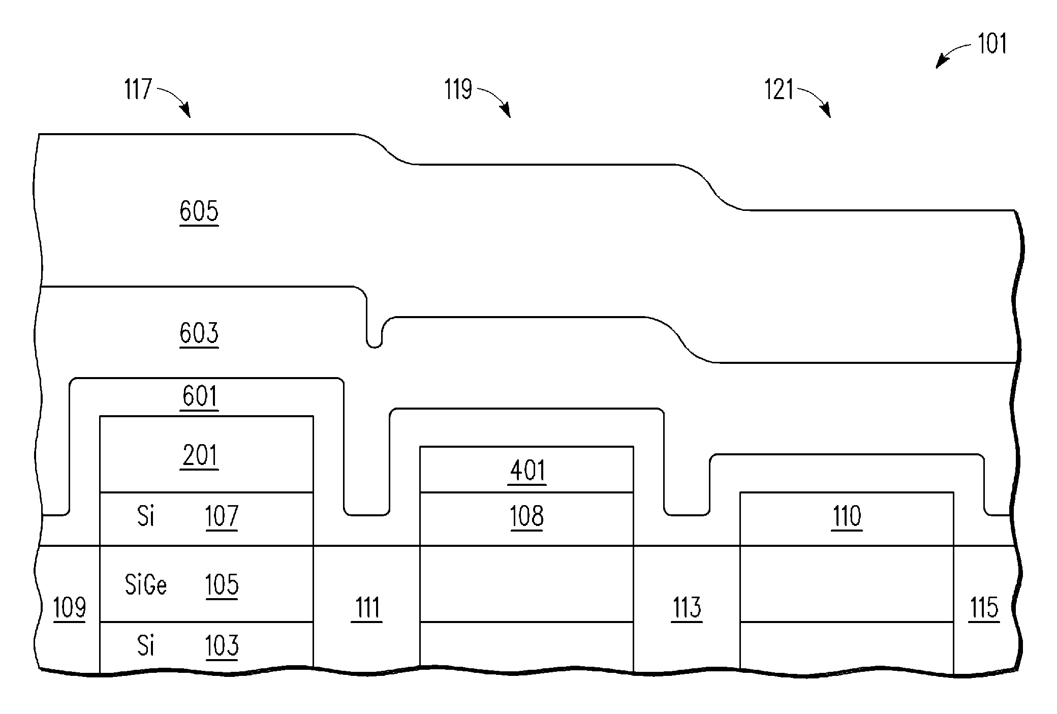
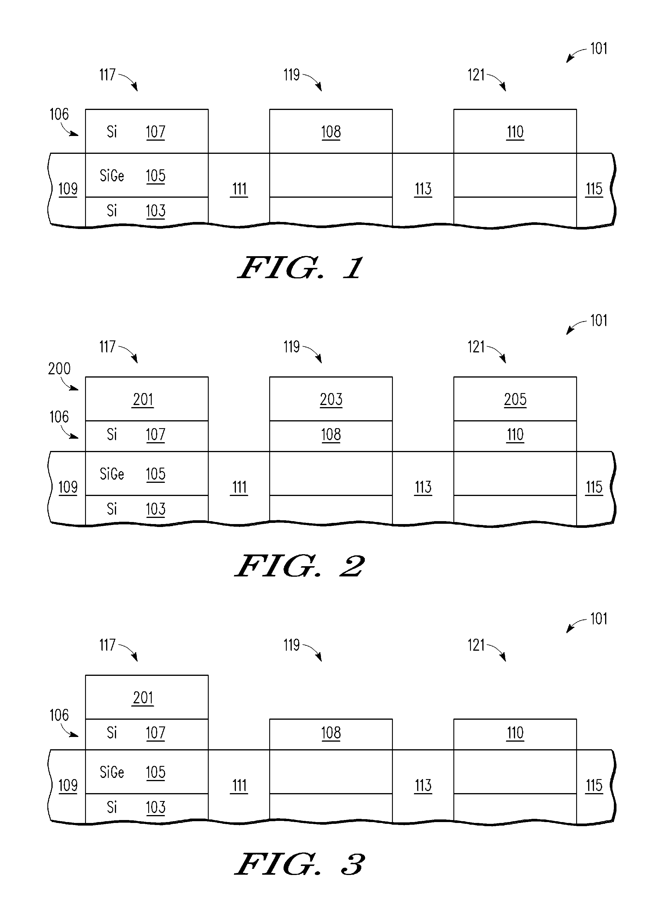
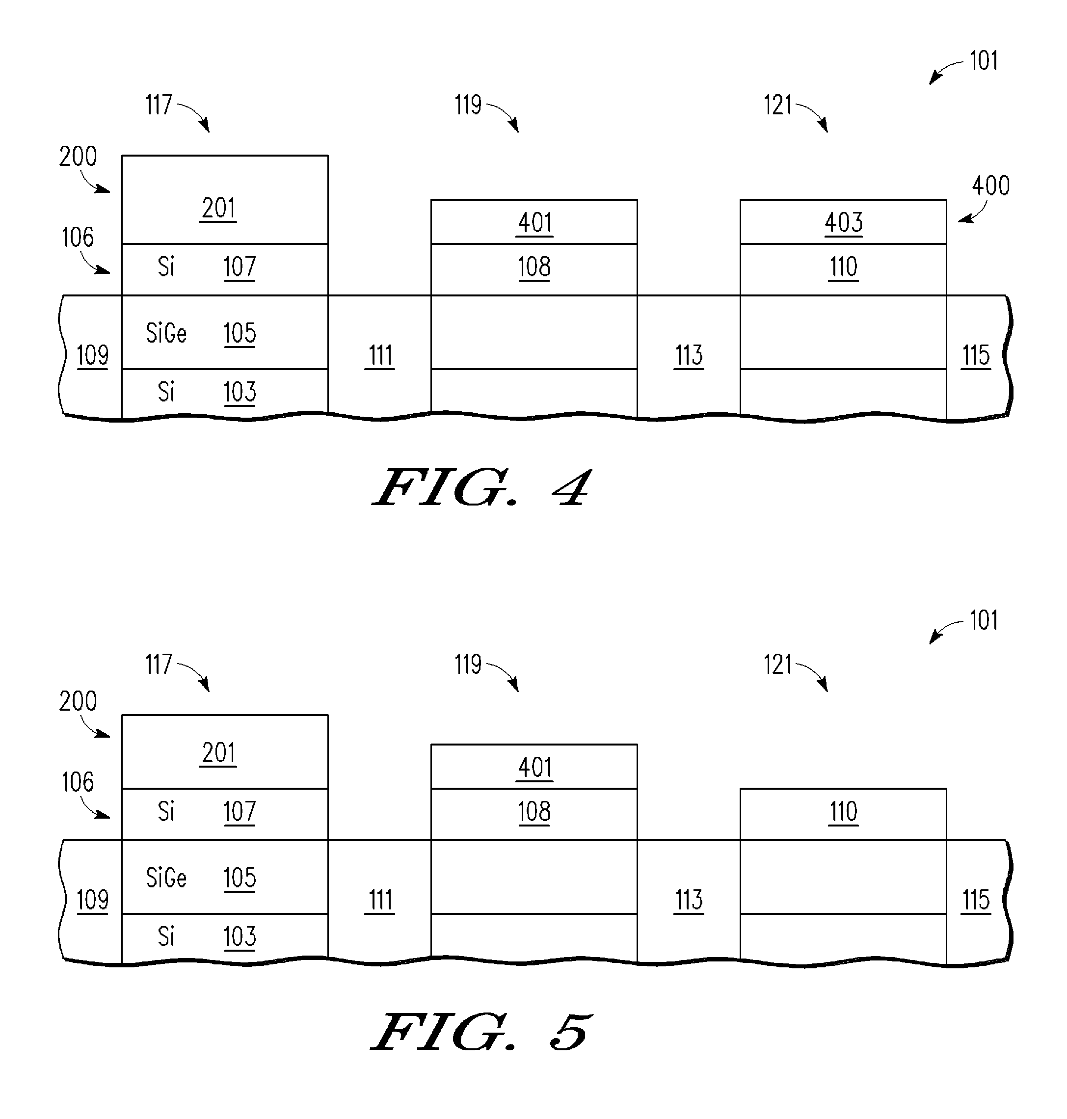
[0010]FIG. 1 is a cutaway side view of wafer 101 used to make semiconductor devices having different dielectric thicknesses in different regions. Shown in FIG. 1 are regions 117, 119, and 121 of wafer 101 in which semiconductor devices of different dielectric thicknesses will be formed. Wafer 101 includes a silicon layer 103 which in one embodiment, is monocrystalline silicon. Layer 103 may be a bulk silicon layer or located on an insulator layer such as e.g. with a semiconductor on insulator (SOI) configuration. In the embodiment shown, a layer 105 of monocrystalline silicon germanium is formed on layer 103. In one embodiment, layer 105 is formed by selective epitaxial growth, but may be formed by other processes (e.g. chemical vapor deposition (CVD), physical vapor deposition (PVD)) in...


PUM

PropertyMeasurementUnit
temperatureaaaaaaaaaa
thicknessaaaaaaaaaa

Abstract

An integrated circuit with devices having dielectric layers with different thicknesses. The dielectric layers include a high-k dielectric and some of the dielectric layers include an oxide layer that is formed from an oxidation process. Each device includes a layer including germanium or carbon located underneath the electrode stack of the device. A silicon cap layers is located over the layer including germanium or carbon.

Description

BACKGROUND OF THE INVENTION[0001]1. Field of the Invention[0002]This invention relates in general to semiconductor devices and more specifically to semiconductor devices with different dielectric thicknesses.[0003]2. Description of the Related Art[0004]Some integrated circuits may include semiconductor devices with different dielectric thickness e.g. different gate dielectric thicknesses. For example, some integrated circuits may have high speed circuits operating in a lower voltage domain and I / O circuitry operating at a higher voltage domain. The higher voltage domain requires transistors with thicker gate dielectrics than transistors of the lower voltage domain.[0005]Implementing an integrated circuit with devices of different dielectric thicknesses may be challenging e.g. especially for devices with silicon germanium channels, high dielectric constant (high-k) gate dielectrics, and / or metal gates.BRIEF DESCRIPTION OF THE DRAWINGS[0006]The present invention may be better understo...

Claims


Application Information

Patent Timeline
Patent Type & Authority Patents(United States)
IPC IPC(8): H01L21/8242
CPCH01L21/823807H01L21/823857H01L29/1054H01L27/092
Inventor KARVE, GAURI V.HALL, MARK D.SAMAVEDAM, SRIKANTH B.
Owner NXP USA INC
Why Eureka
Try Eureka