Charged particle beam writing method and apparatus therefor
a writing method and charge technology, applied in the field of charge particle beam writing method and charge particle beam writing apparatus, can solve the problems of delay in writing time and writing tim
- Summary
- Abstract
- Description
- Claims
- Application Information
AI Technical Summary
Benefits of technology
Problems solved by technology
Method used
Image


Examples
embodiment 1
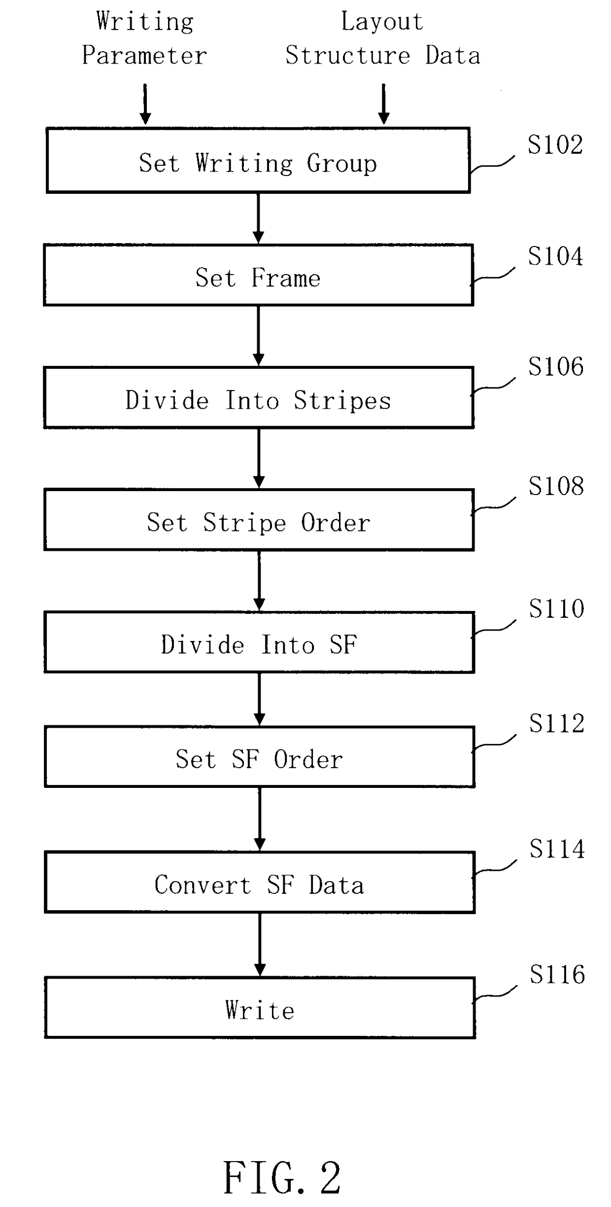
[0023]FIG. 1 is a schematic diagram showing an example of the structure of a writing apparatus according to Embodiment 1. In FIG. 1, a writing apparatus 100 includes a writing unit 150 and a control unit 160. The writing apparatus 100 is an example of a charged particle beam writing apparatus. Particularly, it is an example of the variable-shaped writing apparatus. The writing unit 150 includes an electron lens barrel 102 and a writing chamber 103. In the electron lens barrel 102, there are arranged an electron gun assembly 201, an illumination lens 202, a first aperture plate 203, a projection lens 204, a deflector 205, a second aperture plate 206, an objective lens 207, a main deflector 208, and a sub-deflector 209. In the writing chamber 103, there is arranged an XY stage 105, on which a target workpiece 101, such as a mask, serving as a writing object is placed. The target workpiece 101 is, for example, a photomask used for exposure in manufacturing semiconductor devices. The ta...
embodiment 2
[0051]In Embodiment 1, SF is set for each writing group but it is not limited thereto. In Embodiment 2, the case of setting SF by other method will be described. In Embodiment 2, the apparatus structure is the same as that in FIG. 1, each step of the writing method is the same as that in FIG. 2, and the content of each step is the same as that described in Embodiment 1 except for the points described below.
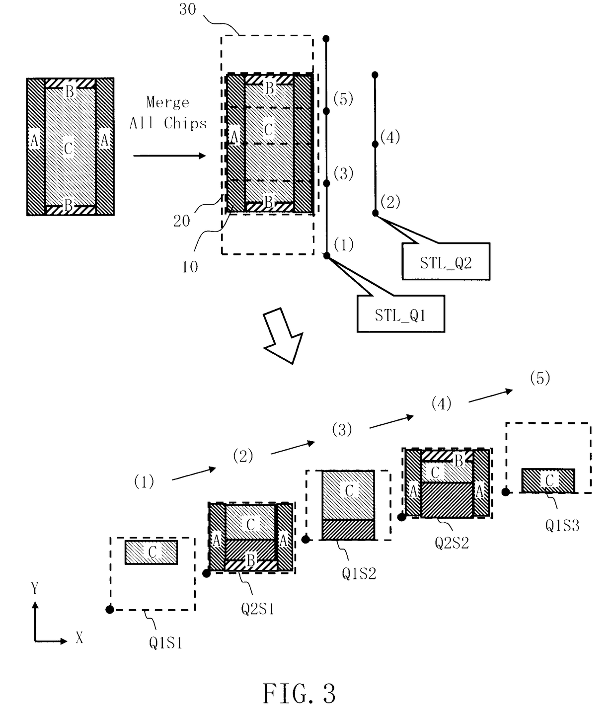
[0052]FIG. 8 is a schematic diagram showing a stripe region and a divided subfield (SF) according to Embodiment 2. In FIG. 8, stripe regions and divided subfields (SFs) of FIG. 3 are shown.
[0053]In S110, as the SF dividing step, the SF dividing unit 132 (small region dividing unit) divides a plurality of stripe regions into a plurality of SFs (small regions). In Embodiment 2, even a stripe region where chips of different writing groups are intermingled is divided, as one SF layer, into a plurality of SFs (small regions) regardless of writing groups. Then, the SF dividing unit 132 ...
PUM
 Abstract
Description
Claims
Application Information
 - R&D
- Intellectual Property
- Life Sciences
- Materials
- Tech Scout
- Unparalleled Data Quality
- Higher Quality Content
- 60% Fewer Hallucinations
Browse by: Latest US Patents, China's latest patents, Technical Efficacy Thesaurus, Application Domain, Technology Topic, Popular Technical Reports.
© 2025 PatSnap. All rights reserved.Legal|Privacy policy|Modern Slavery Act Transparency Statement|Sitemap|About US| Contact US: help@patsnap.com