

Wiring substrate and method of manufacturing the same
a wiring substrate and manufacturing method technology, applied in the direction of printed circuit manufacturing, printed circuit aspects, metallic pattern materials, etc., can solve the problems of deterioration of reliability of connection portions and difficulty in adjusting the amount of solder, and achieve the effect of improving the reliability of the wiring substra
- Summary
- Abstract
- Description
- Claims
- Application Information
AI Technical Summary
Benefits of technology
Problems solved by technology
Method used
Image

Examples
first embodiment
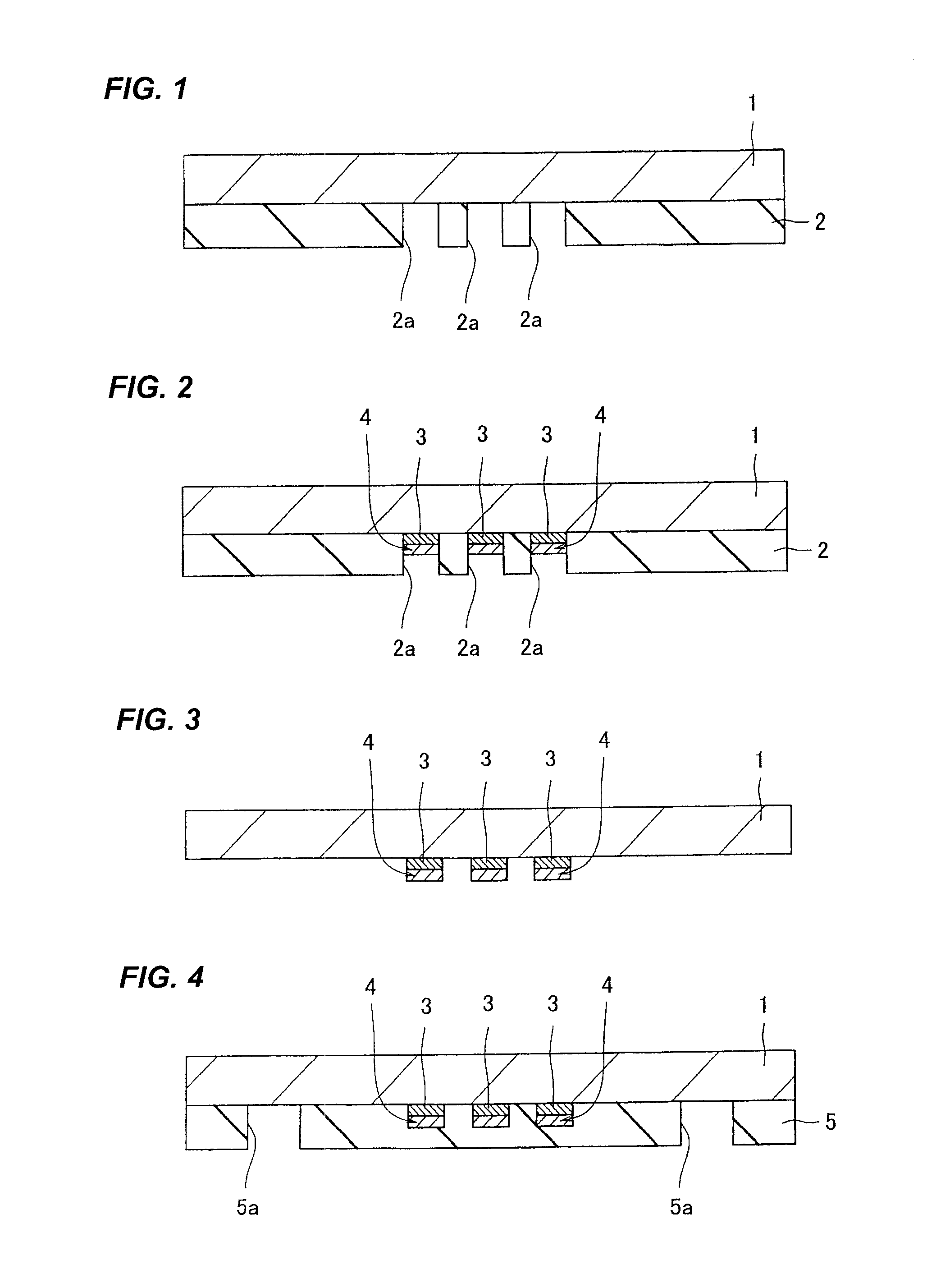
[0068]A method of manufacturing a semiconductor package of this embodiment will be described with reference to the drawings. First, as shown in FIG. 1, a resist layer 2 (plated resist layer) having openings 2a is formed on a conductive support plate 1. The conductive support plate 1 is, for example, a Cu (copper) foil having a thickness of about 500 μm. The resist layer 2 is formed of, for example, dry film resist or liquid resist having a predetermined thickness. For example, dry film resist is formed on the support plate 1, and exposure and development is carried out for the dry film resist. Thus, the resist layer 2 having the openings 2a is formed on the support plate 1.
[0069]The support plate 1 may be formed of a different material, such as an Al (aluminum) foil, insofar as the material is conductive. According to this embodiment, this is because, in a subsequent step, an electrolytic plating method is carried out using the support plate 1 as a plating conduction plate. The supp...
second embodiment
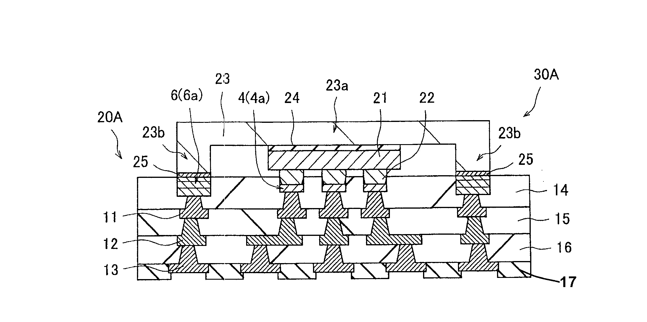
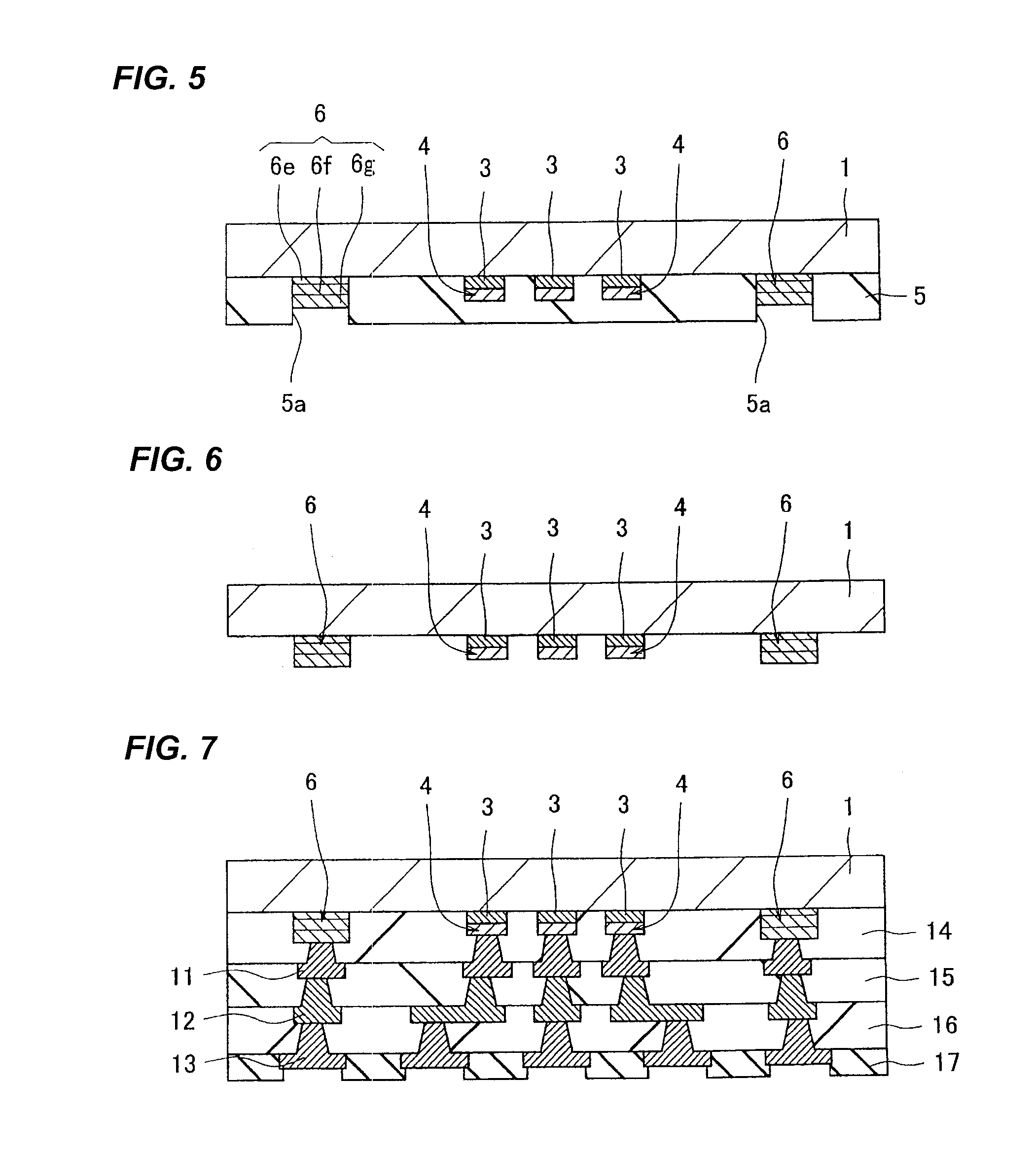
[0112]In the first embodiment, as shown in FIG. 9, a case has been described where, in the region B at the peripheral portion of the wiring substrate 20A, the exposed surfaces of the electrode pads 6a are flush with the surface of the insulating interlayer 14. In this embodiment, as shown in FIG. 16, a case will be described where, in a region B at the peripheral portion of a wiring substrate 20B, the exposed surfaces of electrode pads 6a are flush with the bottom of concave portions 42 formed in the insulating interlayer 14. Overlapping description between the foregoing embodiment and this embodiment may be omitted hereinafter.
[0113]A method of manufacturing a semiconductor package of this embodiment will be described with reference to the drawings. After the manufacturing process of the first embodiment described with reference FIGS. 1 to 4, as shown in FIG. 13, a depth adjusting film 41 of the same material as the support plate 1 is formed on the support plate 1 at the openings 5...
third embodiment
[0127]In the first embodiment, as shown in FIG. 9, a case has been described where, in the region A at the central portion of the wiring substrate 20A, the exposed surfaces of the electrode pads 4a are flush with the bottom of the concave portions 18 formed in the insulating interlayer 14, and in the region B at the peripheral portion of the wiring substrate 20A, the exposed surfaces of the electrode pads 6a are flush with the surface of the insulating interlayer 14. In this embodiment, as shown in FIG. 22, a case will be described where, in a region B at the peripheral portion of a wiring substrate 20C, the exposed surfaces of the electrode pads 4a are flush with the bottom of the concave portions 18 formed in the insulating interlayer 14, and in a region A at the central portion of the wiring substrate 20C, the exposed surfaces of the electrode pads 6a are flush with the surface of the insulating interlayer 14. Overlapping description between the foregoing embodiments and this emb...
PUM
 Abstract
Description
Claims
Application Information