
Imaging device with a heat dissipating member

a technology of imaging device and heat dissipation member, which is applied in the direction of television system, instrument, exposure control, etc., can solve the problems of difficult to escape the heat generated inside the imaging device to the outside of the imaging device, and the substrate of the irradiation is difficult to be cooled, so as to improve the heat dissipation performance of the imaging device

Inactive Publication Date: 2013-07-09
ORMON CORP
View PDF21 Cites 0 Cited by
  • Summary
  • Abstract
  • Description
  • Claims
  • Application Information

AI Technical Summary

Benefits of technology

The patent improves the way imaging devices handle heat. It aims to make the devices better at dissipating the heat that they generate.

Problems solved by technology

However, the irradiation substrate is hard to be cooled if the irradiation substrate is included in the housing of the imaging device.
For instance, if the imaging device is sealed by the housing to ensure waterproof performance and dust-proof performance, it is difficult to escape the heat generated inside the imaging device to outside the imaging device.

Method used


Image

  • Imaging device with a heat dissipating member
  • Imaging device with a heat dissipating member
  • Imaging device with a heat dissipating member

Examples


Embodiment Construction

[0022]Hereinafter, embodiments of the present invention will be described with reference to the drawings. In embodiments of the invention, numerous specific details are set forth in order to provide a more thorough understanding of the invention. However, it will be apparent to one of ordinary skill in the art that the invention may be practiced without these specific details. In other instances, well-known features have not been described in detail to avoid obscuring the invention. In the following description, the same reference numerals are denoted for the same components. The names and the functions thereof are also the same. Therefore, the detailed description thereon will not be repeated.

[0023]

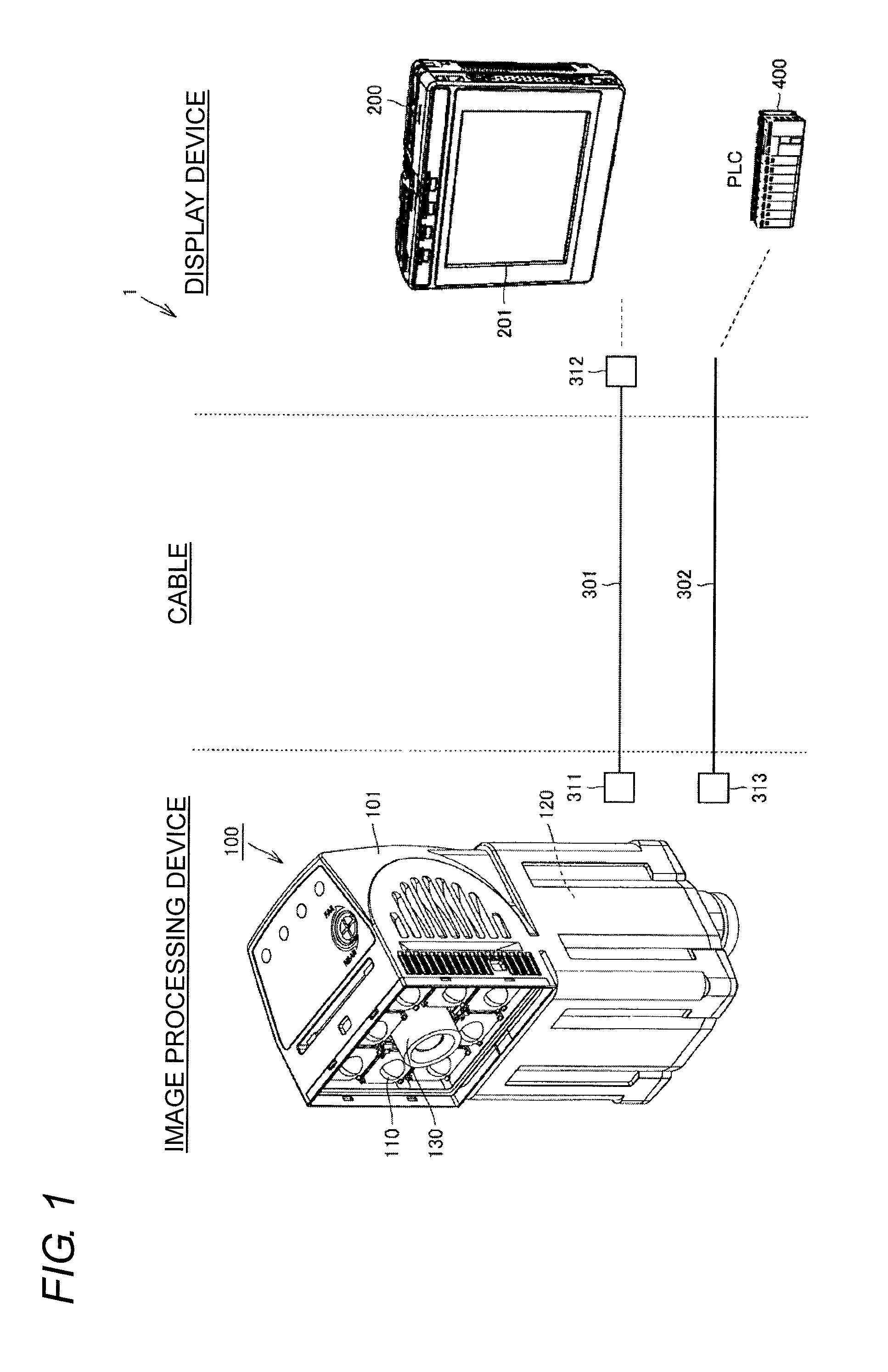
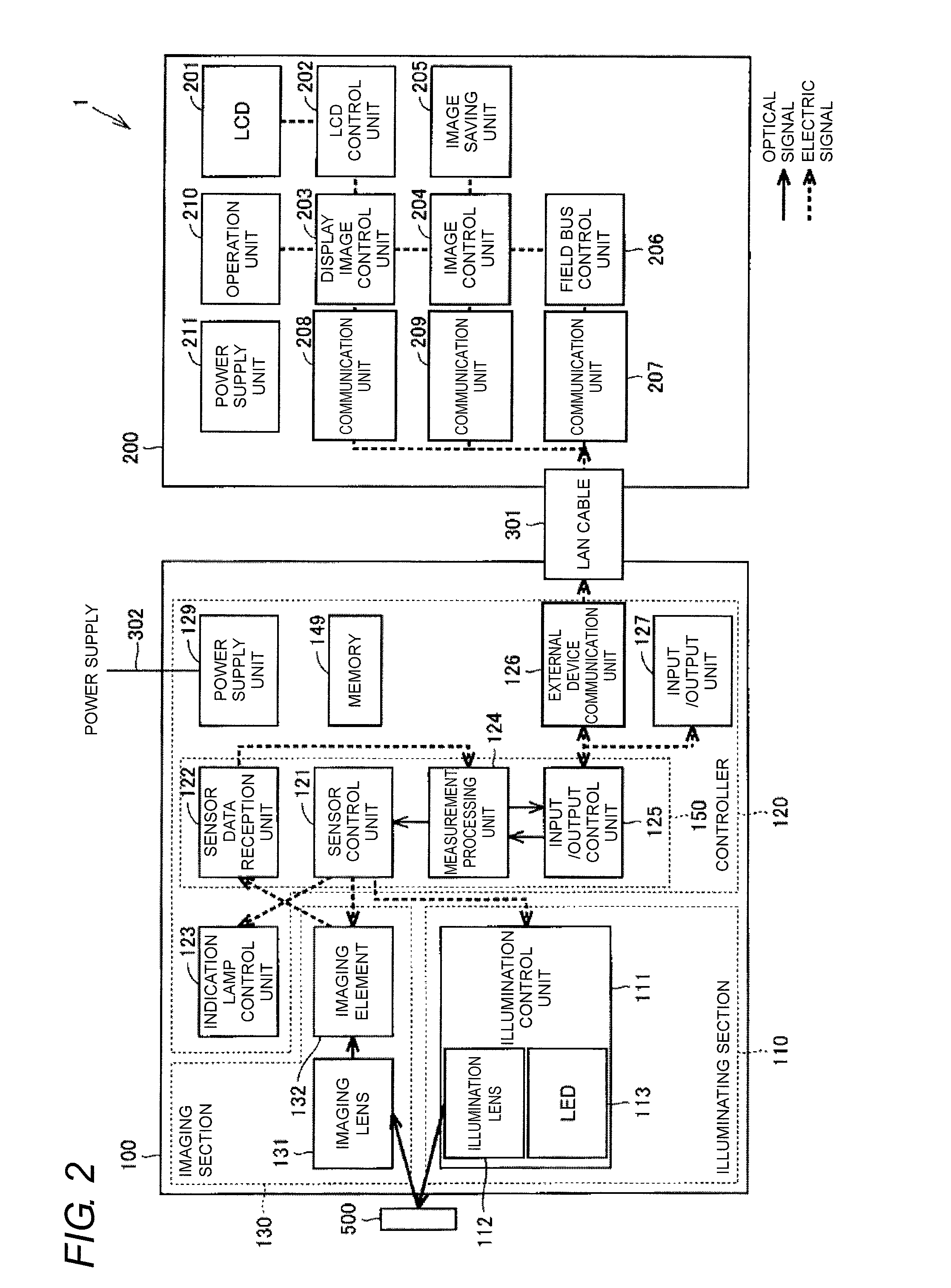
[0024]An image processing device including a controller for processing images will be described as an example of an imaging device. However, the imaging device is not limited to the image processing device including the controller, as hereinafter described. The imaging device is also not...


PUM


Abstract

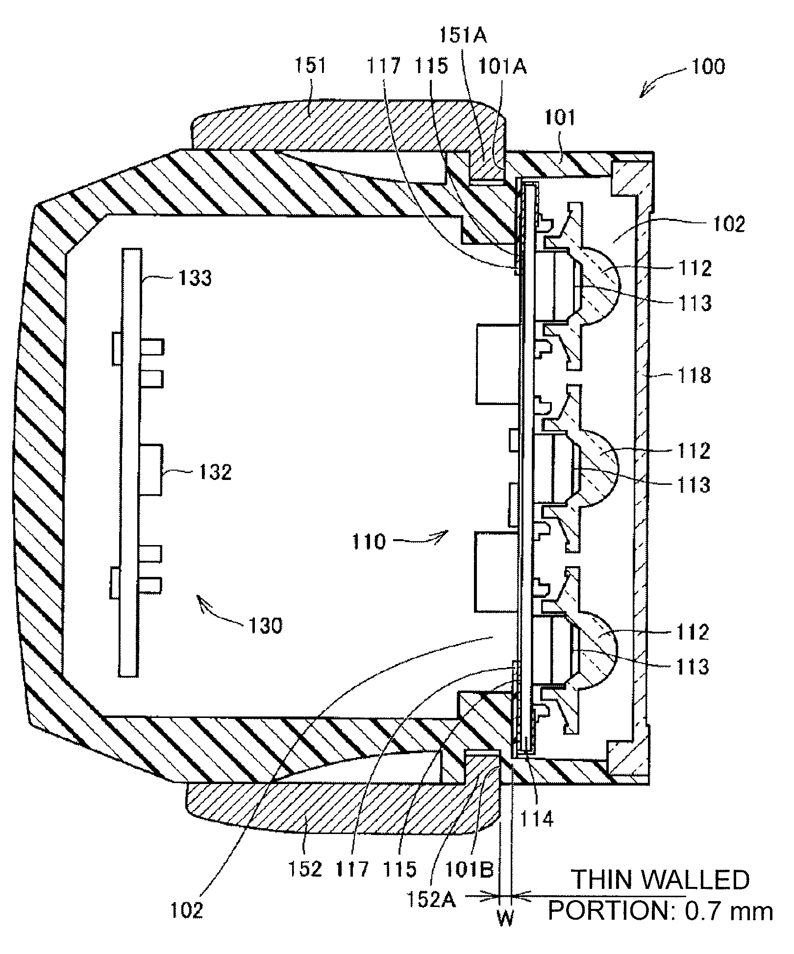
An imaging device has a housing made of a first material having an open region, a first substrate for illumination arranged to cover the open region inside the housing, a second substrate for imaging arranged in parallel to the first substrate inside the housing, and a heat dissipating member made of a second material having a higher heat conductivity than the first material and being attached to a side surface of the housing so as to surround the open region of the housing. A concave is provided at the side surface of the housing, and the heat dissipating member includes a projection that fits to the concave.

Description

1. TECHNICAL FIELD[0001]The present invention relates to imaging devices, and in particular, to an imaging device for irradiating an examining object with light and acquiring an image based on a reflected light from the examining object.2. RELATED ART[0002]In the field of FA (Factory Automation) and the like, various types of image processing techniques are being used from the prior art. For instance, a visual sensor device disclosed in Japanese Unexamined Patent Publication No. 10-320538 is an examination device that targets on a wide variety of objects including small objects such as an electronic component and large objects such as an automobile. In such visual sensor, whether the object is a non-defective product / defective product can be determined by performing an image recognition process on the image data obtained by imaging the object.[0003]Some of such visual sensors include a plurality of light emitting units for emitting light on the examining object such as an LED (Light...

Claims


Application Information

Patent Timeline
Patent Type & Authority Patents(United States)
IPC IPC(8): H04N5/222H04N7/18H04N5/225G03B7/00G03B17/02
CPCG03B21/16H04N5/2252H04N5/2256H05K7/20963H04N23/56H04N23/51
Inventor SUGIYAMA, KOSUKENISHIMORI, NAOKI
Owner ORMON CORP
Learn More