Flash memory device and method of operation

a flash memory and memory cell technology, applied in static storage, digital storage, instruments, etc., can solve the problems of catastrophic data corruption, global erase of all cells in one block, and its entire block being marked as “bad” and other problems, to achieve the effect of reducing the erase voltage, avoiding over-erasing of floating gates, and reducing the overall stress on memory cells

Active Publication Date: 2013-07-16
KIOXIA CORP
View PDF3 Cites 2 Cited by
  • Summary
  • Abstract
  • Description
  • Claims
  • Application Information

AI Technical Summary

Benefits of technology

[0010]According to a second aspect of the invention, a method is provided for operating a NAND flash memory device having a memory cell comprising a floating gate, a control gate connected to a wordline to receive a control voltage therefrom and induce a programming charge on the floating gate, and a bitline adapted to apply an erase voltage to deplete the floating gate of the programming charge. The method entails decreasing the erase voltage if the control voltage is below a threshold level to avoid over-erasing of the floating gate.
[0011]From the above, it should be evident that a technical effect of this invention is the ability to modulating the erase voltage applied to a NAND flash memory cell in order to avoid deep depletion or over-erasing of its floating gate, as well as unnecessary exposures to erase pulses. The result is lower overall stress on the memory cell with the direct effect of higher endurance and the complete avoidance of over-erasing of individual cells.

Problems solved by technology

However, often an undesired side effect is that the global erase of all cells in one block does not take into account any physical variability between the floating gates of the individual cells, nor does it take into account the different levels of charge of the floating gate in the pre-erase state.
If this happens, a nominal programming charge (electron injection) into the floating gate through the control gate will typically result in a “stuck bit,” that is, a very slow-to-program cell that can result in the cell and, by extension, its entire block being marked as “bad.”
In this case, over-erasing of individual cells can result in catastrophic corruption of data.

Method used


Image

  • Flash memory device and method of operation
  • Flash memory device and method of operation
  • Flash memory device and method of operation

Examples


Embodiment Construction

[0016]The present invention is generally applicable to computers and other processing apparatuses that utilize or are capable of using nonvolatile (permanent) memory-based mass storage devices, and more particularly to solid-state drives (SSDs) that make use of NAND flash memory devices.

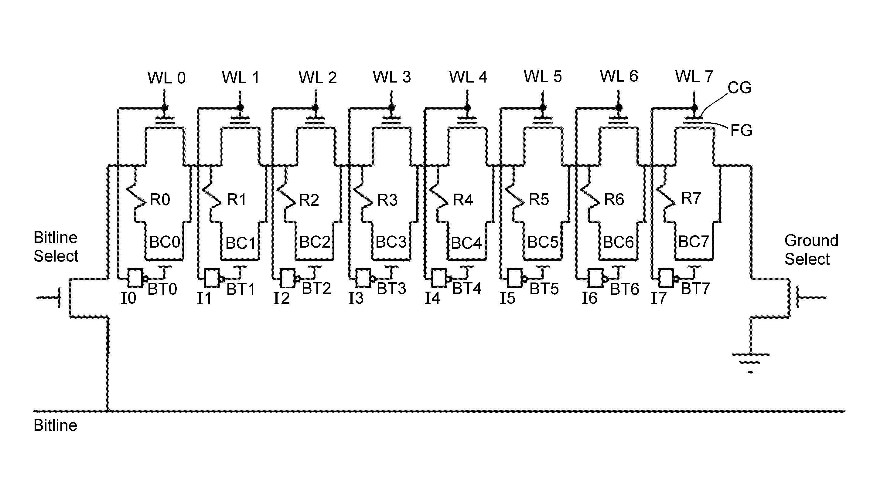
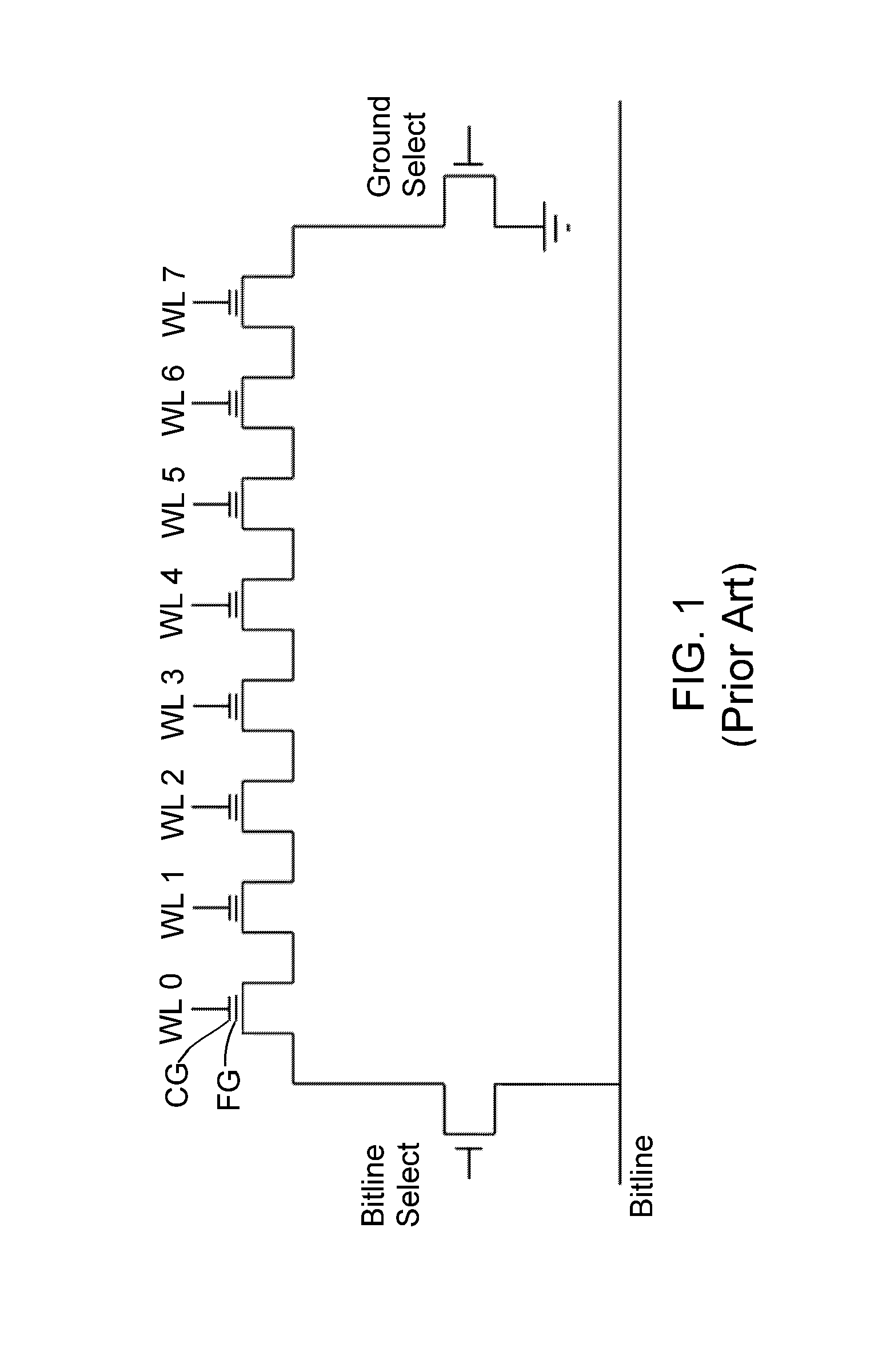
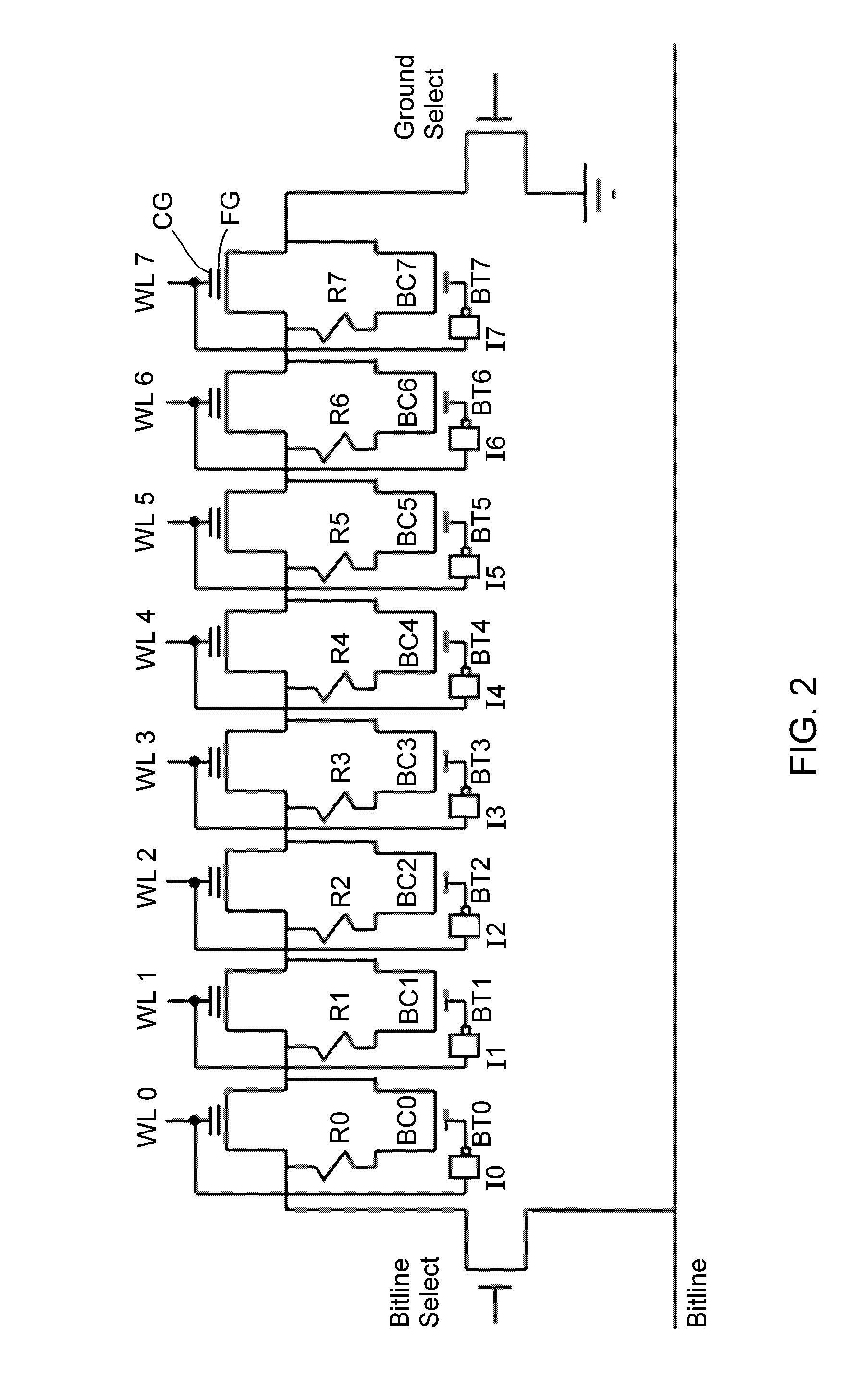
[0017]As discussed above, a conventional NAND flash memory device is erased by subjecting an entire block (containing pages of memory cells) to an erase voltage, typically 20V. As was discussed in reference to FIG. 1, the erase voltage is applied to all serial chains of gates forming a block after the chain a serial chain of gates forming a page after the page has been selected using a “Bitline Select” transistor to apply the erase voltage to the Bitline. All cells within the block are treated equally and subjected to the same Fowler-Nordheim field, regardless of the existing level of charge distribution in the floating gates of the individual cells. Depending on the particular design of the NAND fla...


PUM


Abstract

A NAND flash memory device and method of erasing memory cells thereof, wherein each cell is only subjected to the level of erase voltage needed to restore its nominal “erased” state. Each memory cell of the NAND flash memory device comprises a floating gate, a control gate connected to a wordline and receives a control voltage therefrom to induce a programming charge on the floating gate, and a bitline adapted to apply an erase voltage to deplete the floating gate of the programming charge. Each memory cell further includes circuitry for modulating the erase voltage according to the level of the programming charge on its floating gate.

Description

CROSS REFERENCE TO RELATED APPLICATIONS[0001]This application claims the benefit of U.S. Provisional Application No. 61 / 324,974 filed Apr. 16, 2010. The contents of this prior application are incorporated herein by reference.BACKGROUND OF THE INVENTION[0002]The present invention generally relates to flash memory devices. More particularly, this invention relates to a method and circuitry for the erasing of flash memory cells in order to reduce stress conditions on the tunnel oxide layer of the memory cells and to prevent over-erasing of the memory cells. The erase current is adjusted on a per-cell basis and uses the state of the cell's floating gate to control the erase charge.[0003]As known in the art, flash memory is a type of nonvolatile solid-state memory technology. Flash memory components store information in an array of floating-gate transistors, referred to as cells. NAND flash cells are organized in what are commonly referred to as pages, which in turn are organized in pred...

Claims


Application Information

Patent Timeline
Patent Type & Authority Patents(United States)
IPC IPC(8): G11C16/04
CPCG11C16/0483G11C16/14
Inventor SCHUETTE, FRANZ MICHAEL
Owner KIOXIA CORP
Why Eureka
Try Eureka