Semiconductor display device

a display device and semiconductor technology, applied in the direction of instruments, television systems, television system scanning details, etc., can solve the problems of reducing the area occupied by the driver circuit, reducing yield and cost, and not all semiconductor elements in the signal line driver circuit are required, etc., to achieve high withstand voltage, high speed operation, and high withstand voltage

Active Publication Date: 2013-08-27
SEMICON ENERGY LAB CO LTD
View PDF148 Cites 10 Cited by
  • Summary
  • Abstract
  • Description
  • Claims
  • Application Information

AI Technical Summary

Benefits of technology

[0008]However, not all semiconductor elements included in the signal line driver circuit are required to have the above level of withstand voltage. For example, a circuit distant from the output side of the signal line driver circuit, such as a shift register, only needs to withstand a voltage of approximately 3 V at most. As for a semiconductor element used in the shift register, high-speed operation is more important than high withstand voltage to secure high quality of a display image of the semiconductor display device. In order to realize high-speed operation, it is preferable that the semiconductor element be miniaturized and the thickness of the insulating films thereof be reduced.
[0010]In view of the above problems, an object of the present invention is to provide a semiconductor display device including a driver circuit whose high-speed operation and high withstand voltage are secured without making the manufacturing process complicated. Another object of the present invention is to provide a semiconductor display device including a driver circuit whose power consumption is suppressed and whose high withstand voltage is secured without making the manufacturing process complicated. Another object of the present invention is to provide a semiconductor display device including a driver circuit whose occupation area is reduced and whose high withstand voltage is secured without making the manufacturing process complicated.
[0012]As semiconductors having a wider bandgap and lower intrinsic carrier density than silicon or germanium, an oxide semiconductor, silicon carbide, gallium nitride, and the like can be given. The bandgap of an oxide semiconductor, the bandgap of silicon carbide, and the bandgap of gallium nitride are 3.0 eV to 3.5 eV, 3.26 eV, and 3.39 eV, respectively, which are approximately three times as wide as that of silicon. The wide bandgaps of these semiconductors are advantageous in terms of improvement in withstand voltage of a semiconductor element such as a transistor, a reduction in loss of power, and the like. According to an embodiment of the present invention, with the use of the above-described semiconductor having a wide bandgap in the circuit which needs to have high withstand voltage, a semiconductor element having resistance to intermediate voltage, that is, intermediate withstand voltage can be manufactured.
[0013]According to an embodiment of the present invention, the circuit which does not need to have such high withstand voltage can be formed using a semiconductor and a process different from those of the circuit which needs to have high withstand voltage. Therefore, in the circuit which does not need to have such high withstand voltage, a semiconductor element can be manufactured so as to have resistance to low voltage, that is, low withstand voltage, to operate at high speed, and to be miniaturized with the thickness of an insulating film thereof reduced.
[0014]That is, according to an embodiment of the present invention, semiconductor elements having structures most suitable for characteristics needed for circuits can be separately manufactured without making the process complicated.
[0020]With the above structure, according to an embodiment of the present invention, a semiconductor display device including a driver circuit whose high-speed operation and high withstand voltage are secured without making the manufacturing process complicated can be provided. With the above structure, according to an embodiment of the present invention, a semiconductor display device including a driver circuit whose power consumption is suppressed and whose high withstand voltage is secured without making the manufacturing process complicated can be provided. With the above structure, according to an embodiment of the present invention, a semiconductor display device including a driver circuit whose occupation area is reduced and whose high withstand voltage is secured without making the manufacturing process complicated can be provided.

Problems solved by technology

However, not all semiconductor elements included in the signal line driver circuit are required to have the above level of withstand voltage.
It is necessary to employ a complicated process in order to manufacture semiconductor elements having different structures through the same process, which results in a reduction in yield and an increase in cost.
Accordingly, a reduction in the area occupied by the driver circuit is hindered, and it is difficult to secure high operation speed and to suppress power consumption.

Method used


Image

  • Semiconductor display device
  • Semiconductor display device
  • Semiconductor display device

Examples


embodiment 1

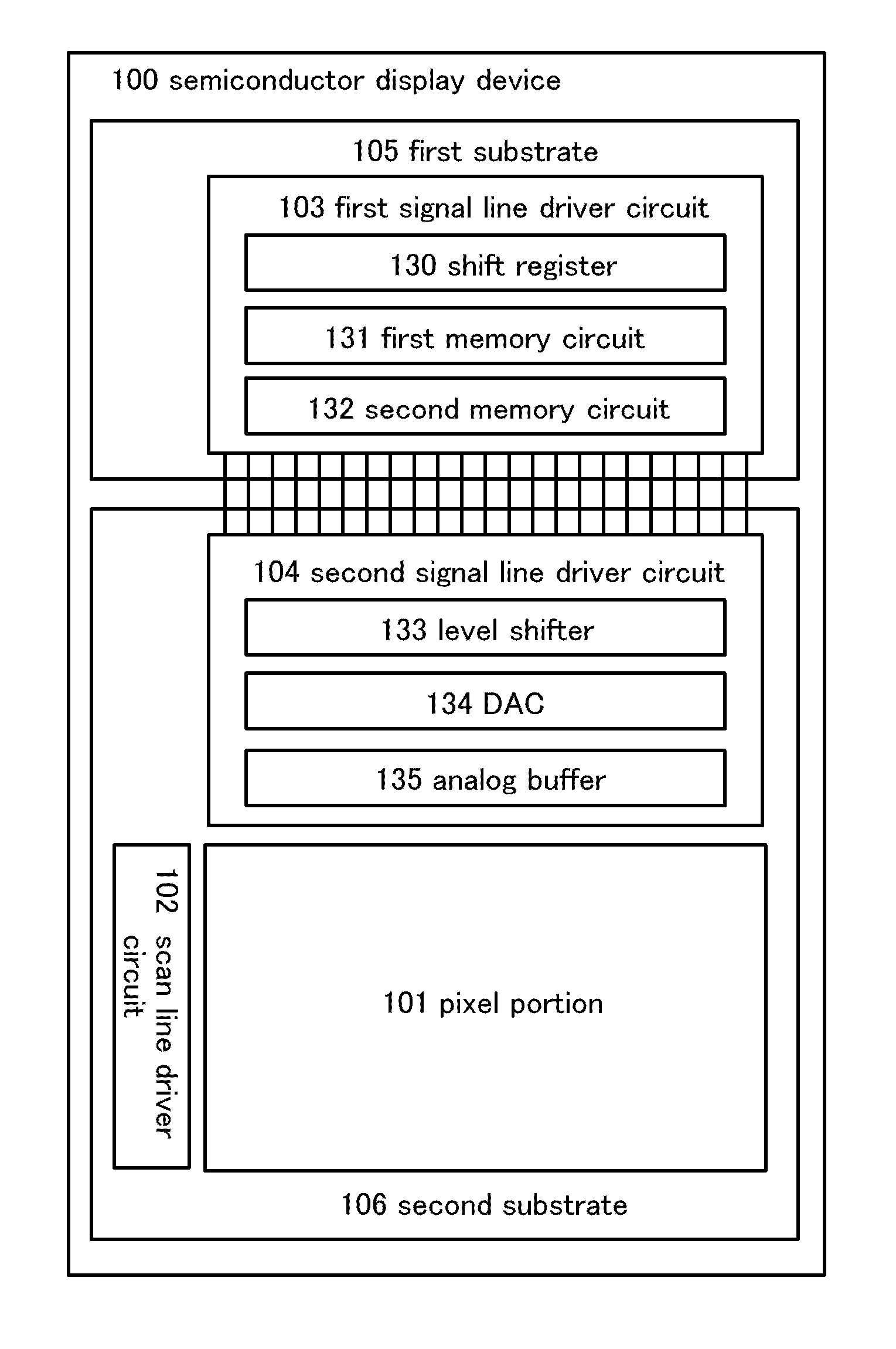
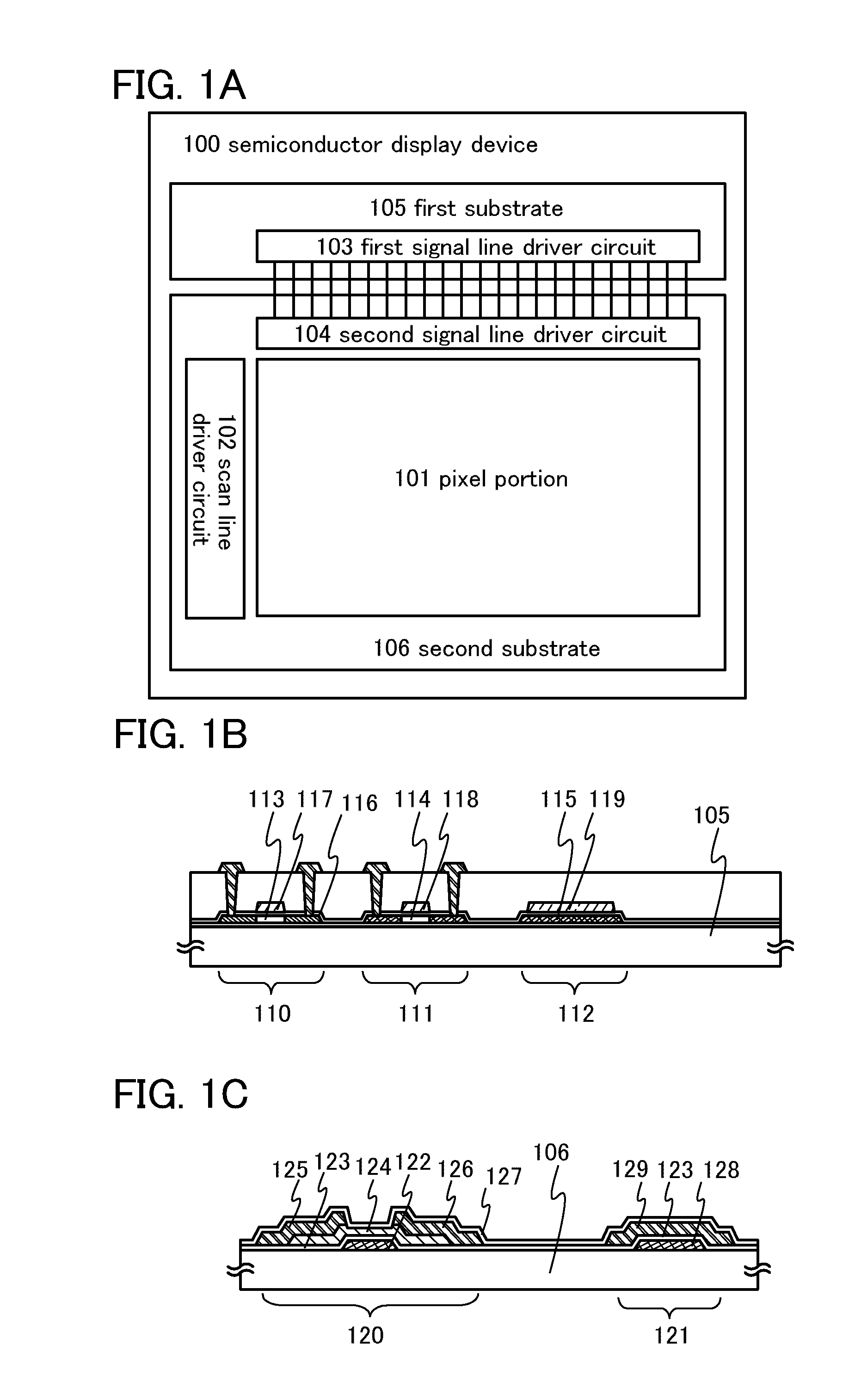
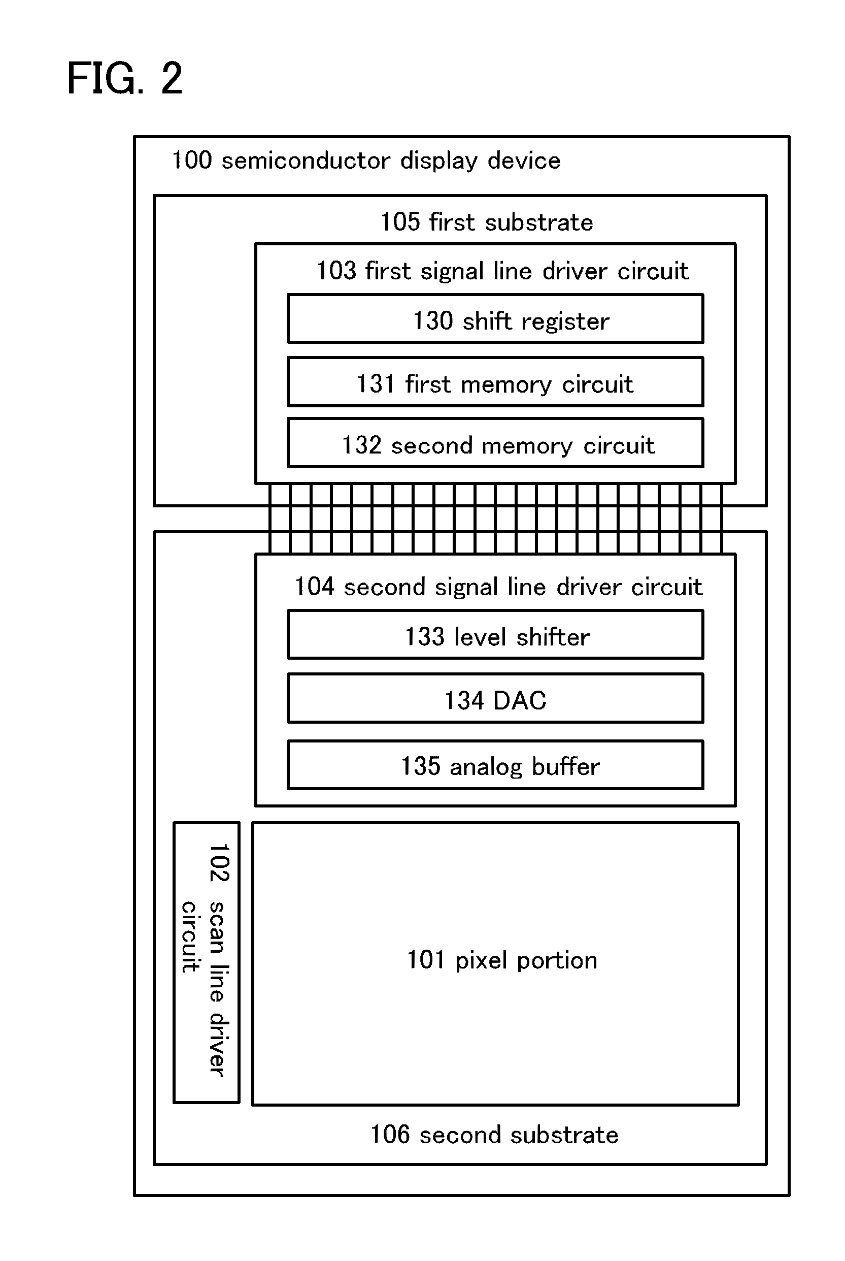
[0044]FIG. 1A is a block diagram illustrating an example of a structure of a semiconductor display device according to an embodiment of the present invention. A semiconductor display device 100 illustrated in FIG. 1A includes a pixel portion 101 where a display element is provided in each pixel, and driver circuits that control the operation of the pixel portion 101.

[0045]In FIG. 1A, the driver circuits correspond to a scan line driver circuit 102, a first signal line driver circuit 103, and a second signal line driver circuit 104. Specifically, the scan line driver circuit 102 selects a pixel included in the pixel portion 101. The first signal line driver circuit 103 and the second signal line driver circuit 104 supply a video signal to the pixel selected by the scan line driver circuit 102.

[0046]The first signal line driver circuit 103 includes a circuit that controls the timing of sampling serially input video signals and needs to have high operation speed rather than high withst...

embodiment 2

[0083]In this embodiment, specific configurations of a level shifter, a DAC, and a buffer used in a second signal line driver circuit will be described.

[0084]FIG. 6 illustrates an example of a level shifter including an n-channel transistor. The level shifter illustrated in FIG. 6 includes a bootstrap circuit as a base. Specifically, the level shifter illustrated in FIG. 6 includes bootstrap circuits 600a to 600c, a transistor 601, and a transistor 602.

[0085]A drain electrode and a gate electrode of the transistor 602 are connected to a node supplied with a high-level power supply potential VDD1, and a source electrode of the transistor 602 is connected to a drain electrode of the transistor 601. A potential of an input signal IN to be input to the level shifter is supplied to a gate electrode of the transistor 601, and a source electrode of the transistor 601 is connected to a node supplied with a low-level power supply potential VSS.

[0086]The bootstrap circuit 600a includes a tran...

embodiment 3

[0113]In this embodiment, a specific structure of a pixel portion will be described by taking a liquid crystal display device which is one of semiconductor display devices of the present invention as an example.

[0114]FIG. 9 illustrates a configuration of a pixel portion 301 including a plurality of pixels 300, as an example. In FIG. 9, each of the pixels 300 includes at least one of signal lines S1 to Sx and at least one of scan lines G1 to Gy. In addition, the pixel 300 includes a transistor 305 which functions as a switching element, a liquid crystal element 306, and a capacitor 307. The liquid crystal element 306 includes a pixel electrode, a counter electrode, and liquid crystals to which voltage between the pixel electrode and the counter electrode is applied.

[0115]The transistor 305 controls whether a potential of the signal line, that is, a potential of a video signal is supplied to the pixel electrode of the liquid crystal element 306. A predetermined potential is supplied t...


PUM


Abstract

A semiconductor display device comprising a pixel portion and a signal line driver circuit comprising a first circuit, a second circuit configured to control timing of the sampled serial video signals by the first circuit, and a third circuit configured to perform signal processing on the parallel video signals, wherein the second circuit comprises a first semiconductor element formed over a first substrate, the first semiconductor element including a first semiconductor layer, wherein the third circuit comprises a second semiconductor element formed over a second substrate, the second semiconductor element including a second semiconductor layer, wherein the pixel portion comprises a third semiconductor element formed over the second substrate, the third semiconductor element including a third semiconductor layer, wherein the first semiconductor layer comprises silicon or germanium, and wherein each the second semiconductor layer and the third semiconductor layer has a wider bandgap than the first semiconductor layer.

Description

TECHNICAL FIELD[0001]The present invention relates to a semiconductor display device including a driver circuit.BACKGROUND ART[0002]A semiconductor display device in which a transistor including amorphous silicon is provided in a pixel portion has advantages of high productivity and low cost because the semiconductor display device is applicable to a glass substrate of the fifth generation (1200 mm long×1300 mm wide) or higher generations. Further, in the semiconductor display device, a driver circuit such as a scan line driver circuit for selecting a pixel or a signal line driver circuit for supplying a video signal to the selected pixel is required to operate at high speed. Therefore, the driver circuit is formed using crystalline silicon such as single crystal silicon, which has higher mobility than amorphous silicon.[0003]In general, an IC chip including a driver circuit formed using a single crystal silicon wafer or the like is mounted in the periphery of a pixel portion formed...

Claims


Application Information

Patent Timeline
Patent Type & Authority Patents(United States)
IPC IPC(8): G09G5/00
CPCG09G3/3688G09G2300/0417
Inventor YAMAZAKI, SHUNPEIKOYAMA, JUN
Owner SEMICON ENERGY LAB CO LTD
Why Eureka
Try Eureka