Semiconductor module and method of manufacturing semiconductor module

a semiconductor module and semiconductor technology, applied in the field of semiconductor modules, can solve the problems of reducing thickness, insulating substrates are more prone to creeping breakdown, and the material type cannot be used to sufficiently so as to reduce the thickness of insulating substrates, reduce the magnitude of electric fields present, and high breakdown voltages

Active Publication Date: 2017-11-14
FUJI ELECTRIC CO LTD
View PDF14 Cites 3 Cited by
  • Summary
  • Abstract
  • Description
  • Claims
  • Application Information

AI Technical Summary

Benefits of technology

[0009]The present invention aims to provide a semiconductor module that alleviates concentration of local electric fields at intersections between the principal surface of an insulating substrate and the side faces of a conductive plate arranged on the principal surface of the insulating substrate and that has an improved dielectric breakdown voltage, as well as a method of manufacturing such a semiconductor module. Accordingly, the present invention is directed to a scheme that substantially obviates one or more of the problems due to limitations and disadvantages of the related art.
[0018]In one aspect of the present invention, when a voltage is applied, the ionic liquid contained in the ion gel moves within the ion gel according to the resulting electric potential gradient and gets distributed near the surface of the first conductive plate and / or near the surface of the insulating substrate at the intersections between the first principal surface of the insulating substrate and the side faces of the first conductive plate, thereby terminating local lines of electric force. This alleviates electric field concentration at the intersections and improves the dielectric breakdown voltage. Moreover, this improvement in the dielectric breakdown voltage of the insulating substrate makes it possible to reduce the thickness of the insulating substrate, thereby making it possible to reduce production costs.

Problems solved by technology

In light of the demand for semiconductor modules with increasingly high breakdown voltages in recent years, this type of material cannot be used to sufficiently reduce of the magnitude of the electric fields present.
Moreover, reducing the thickness of the insulating substrate, for example, only makes the insulating substrate more prone to creeping breakdown when exposed to stronger electric fields.
Therefore, the thickness of the insulating substrate cannot be reduced, and meanwhile, using thick insulating substrates results in increased production costs.

Method used


Image

  • Semiconductor module and method of manufacturing semiconductor module
  • Semiconductor module and method of manufacturing semiconductor module
  • Semiconductor module and method of manufacturing semiconductor module

Examples


working examples

[0064]Next, certain aspects of the present invention will be described in more detail using specific working examples. Note, however, that the present invention is not limited in any way by these working examples.

working example 1

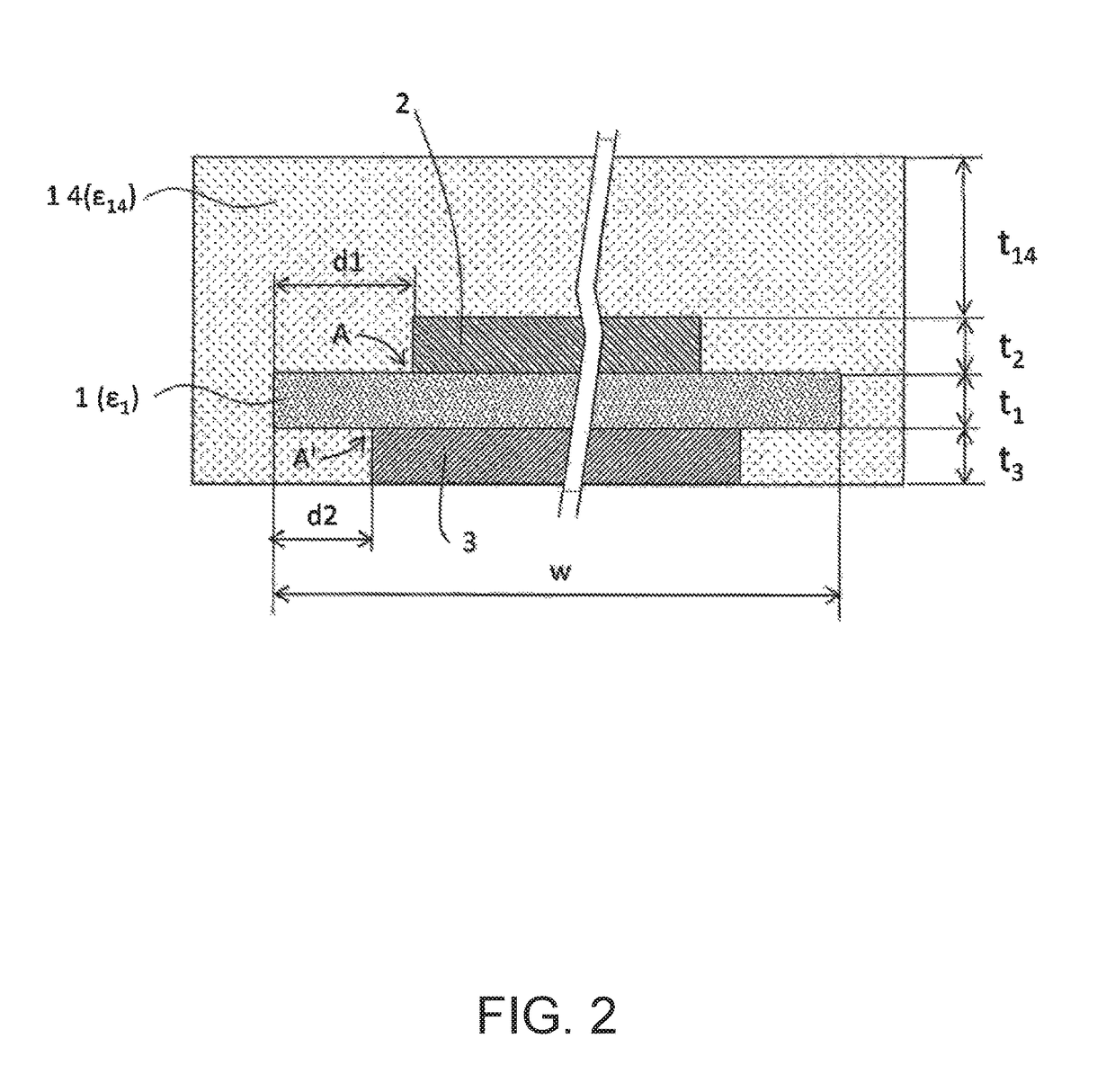
[0065]FIG. 6 is a cross-sectional view illustrating a dielectric breakdown voltage evaluation sample 200. An insulated circuit board 4 (a Denka AlN plate made by Denka Company Limited) in which an Al first conductive plate 2 and an Al second conductive plate 3 both 0.2 mm in thickness were respectively layered on both surfaces of an AlN insulating substrate 1 that was 1 mm in thickness was used. In the insulated circuit board 4, the minimum distance (a first edge distance) from the outer edge of the insulating substrate 1 to the first conductive plate 2 was 1.5 mm, and the minimum distance (a second edge distance) from the outer edge of the insulating substrate 1 to the second conductive plate 3 was 0.5 mm. Next, an ion gel precursor material was prepared by mixing together 1 part by mass 1-ethyl-3-methylimidazolium bis(trifluoromethanesulfonyl)imide (EMIM TFSI) as the ionic liquid, 5 parts by mass a poly(styrene-b-methyl methacrylate-b-styrene) triblock copolymer (PS-PMMA-PS) as th...

working example 2

[0066]Working Example 2 was produced the same as Working Example 1 except in that the thickness of the AlN insulating substrate in the insulated circuit board 4 (a Denka AlN plate made by Denka Company Limited) was set to 0.625 mm.


PUM


Abstract

A semiconductor module includes an insulated circuit board that includes an insulating substrate, a first conductive plate arranged on a first principal surface of the insulating substrate and within the outer edges of the insulating substrate, and a second conductive plate arranged within the outer edges of the insulating substrate on a second principal surface of the insulating substrate that faces the first principal surface. Furthermore, boundary edges between the first principal surface of the insulating substrate and the side faces of the first conductive plate are covered by an ion gel that contains an ionic liquid.

Description

BACKGROUND OF THE INVENTION[0001]Technical Field[0002]The present invention relates to a semiconductor module that includes a power semiconductor device and to a method of manufacturing the semiconductor module.[0003]Background Art[0004]Semiconductor modules that include a power semiconductor device exhibit excellent power conversion efficiency and are widely used in renewable energy fields such as solar power generation and wind power generation, automobiles such as hybrid automobiles and electric automobiles, railway applications such as electric trains, and more. In these types of semiconductor modules, a variety of protective measures are employed not only in the semiconductor device but also in the insulating substrate in order to prevent dielectric breakdown even if high voltages are applied.[0005]Patent Document 1, for example, discloses such a semiconductor device in which a protective treatment is applied to the insulating substrate. This semiconductor device includes a pow...

Claims


Application Information

Patent Timeline
Patent Type & Authority Patents(United States)
IPC IPC(8): H01L23/498H01L23/31H01L21/56H01L21/48H01L23/24H01L23/373H01L23/60H01L23/14H01L25/07H01L23/00
CPCH01L23/49894H01L21/4871H01L21/563H01L23/24H01L23/3121H01L23/3142H01L23/3735H01L23/49811H01L23/60H01L2924/3511H01L2924/181H01L2924/13091H01L2924/13055H01L2924/12032H01L2924/10272H01L2924/10253H01L2924/1033H01L2224/73265H01L2224/73263H01L2224/48464H01L2224/48227H01L2224/48137H01L2224/48091H01L2224/45624H01L2224/45565H01L2224/45147H01L2224/45124H01L2224/4516H01L2224/45015H01L2224/40227H01L23/142H01L24/29H01L24/32H01L24/40H01L24/45H01L24/73H01L25/072H01L2224/291H01L2224/32225H01L2224/40137H01L2924/00014H01L2924/00012H01L2924/014H01L2924/2076H01L23/053H01L2224/83801H01L24/83H01L2224/37099H01L2224/84H01L2224/73221
Inventor KANAI, NAOYUKI
Owner FUJI ELECTRIC CO LTD
Why Eureka
Try Eureka