Liquid crystal device, manufacturing method thereof, and electronic apparatus

a technology of liquid crystal devices and manufacturing methods, applied in non-linear optics, instruments, optics, etc., can solve problems such as degrading aperture ratios, and achieve the effect of sufficient capacity for storage capacitors

Inactive Publication Date: 2009-02-17
EPSON IMAGING DEVICES CORP
View PDF5 Cites 4 Cited by
  • Summary
  • Abstract
  • Description
  • Claims
  • Application Information

AI Technical Summary

Benefits of technology

[0023]An advantage of some aspects of the invention is that it provides a liquid crystal device, a manufacturing method of the liquid crystal device, and an electronic apparatus, each of which can prevent cross talk of a scanning line and a data line, while ensuring a sufficient capacity for a storage capacitor.
[0026]That is, since the switching element is provided below the insulation layer, for instance, when the scanning line and the data line connected to the switching element, and the second insulation layer between the scanning line and the data line are provided below the insulation layer, increase in thickness of the second insulation layer can ensure the interval between the scanning line and the data line, thereby preventing the cross talk from occurring. In addition, decrease in thickness of the insulation layer can ensure a sufficient capacity for the storage capacitor.
[0028]With this configuration, since the pixel electrode in the transmissive region extends to the space between the insulation layer and the liquid crystal thickness adjustment layer to provide the first capacitance electrode, for instance, provision of only a transparent conductive film on the insulation layer can easily provide the pixel electrode in the transmissive region and the first capacitance electrode.

Problems solved by technology

However, the increase in the areas of the two capacitance electrodes may cause the capacitance electrodes to extend beyond the reflective region and thus be exposed to the transmissive region, thereby degrading the aperture ratio.

Method used


Image

  • Liquid crystal device, manufacturing method thereof, and electronic apparatus
  • Liquid crystal device, manufacturing method thereof, and electronic apparatus
  • Liquid crystal device, manufacturing method thereof, and electronic apparatus

Examples


Embodiment Construction

[0050]Hereinafter, an exemplary embodiment of the invention will be described below with reference to accompanying drawings. Note that like numbers reference like elements and like descriptions will be omitted or simplified in the following exemplary embodiment and modifications.

Exemplary Embodiment

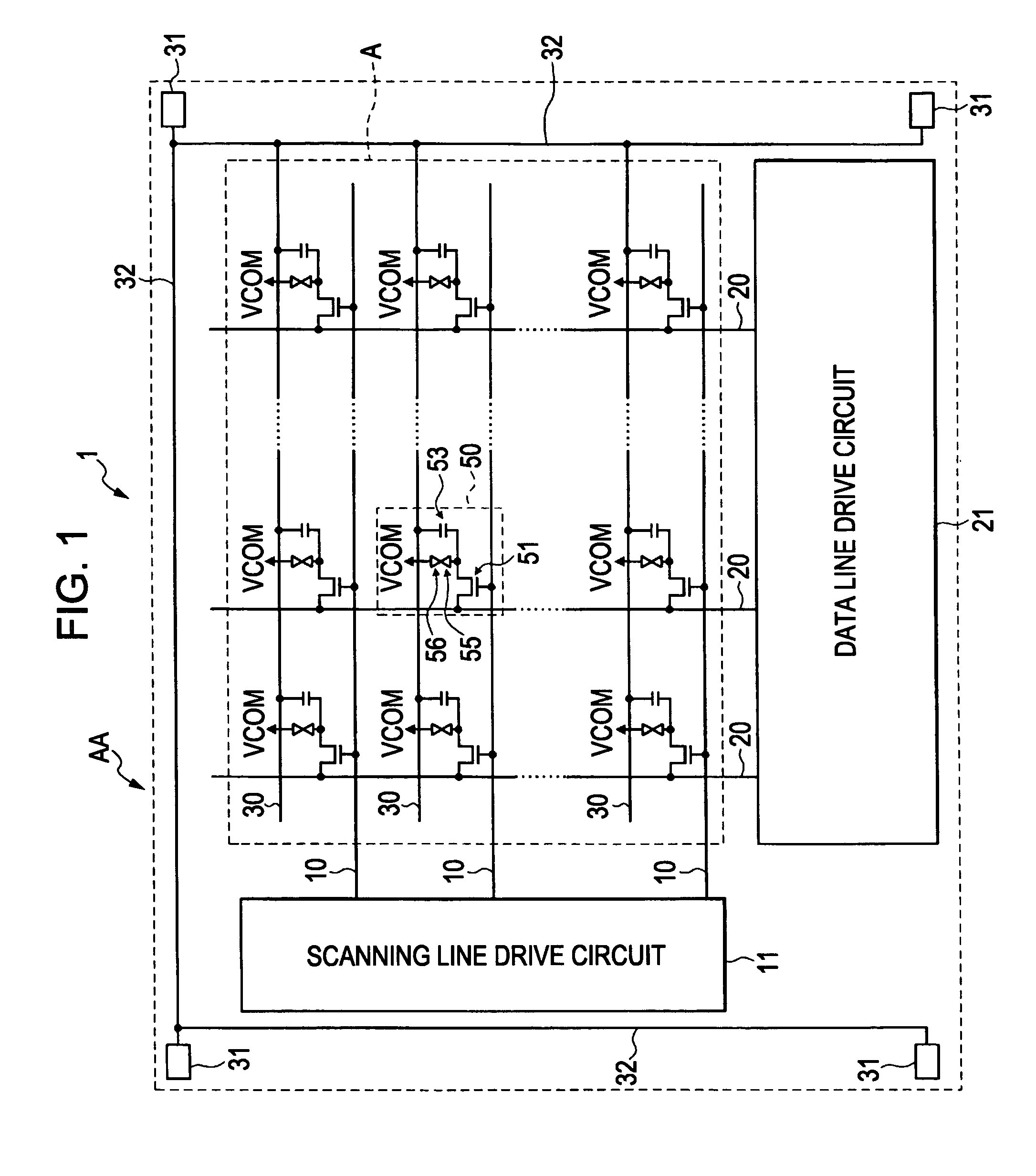
[0051]FIG. 1 is a block diagram of a liquid crystal device 1 according to an exemplary embodiment of the invention.

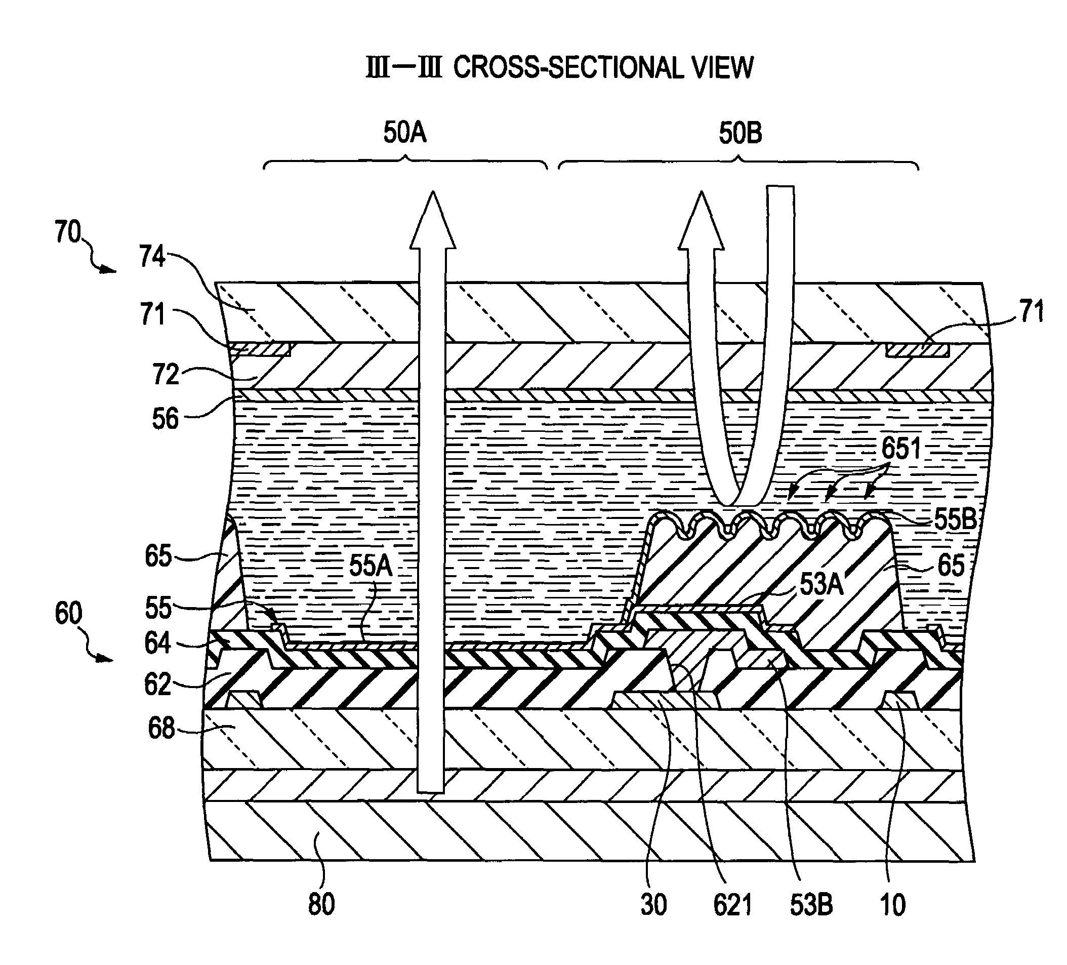
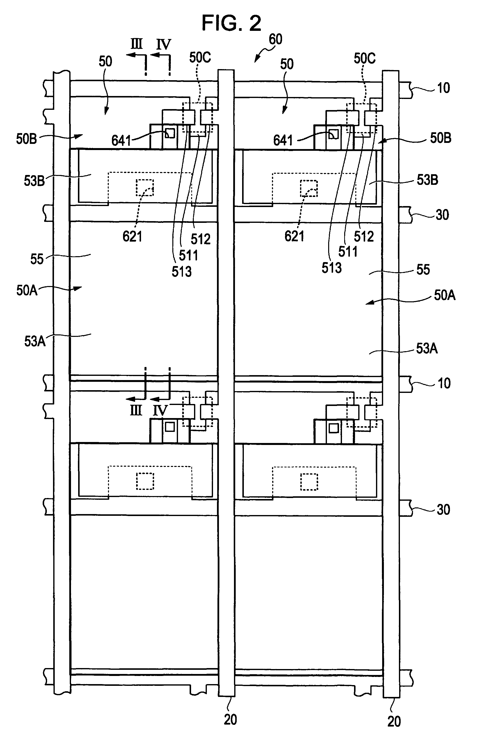
[0052]The liquid crystal device 1 includes a liquid crystal panel AA and a backlight unit as an illumination unit (see FIGS. 4 and 5). The liquid crystal panel AA includes a display region A which is provided with a plurality of pixels 50, and a scanning line drive circuit 11 and a data line drive circuit 21 which are provided in the periphery of the display region A for driving the pixels 50.

[0053]The liquid crystal panel AA includes a plurality of scanning lines 10 and a plurality of common lines (capacitance lines) 30, the scanning lines 10 and the common lines 30 being al...


PUM

PropertyMeasurementUnit
thicknessaaaaaaaaaa
transparentaaaaaaaaaa
electrically conductiveaaaaaaaaaa

Abstract

A liquid crystal device includes: a first substrate including a scanning line, a data line, a switching element, a pixel electrode and a storage capacitor associated with an intersection of the scanning line and the data line; a second substrate; and liquid crystal interposed between the substrates. A region where the pixel electrode is provided includes a reflective region and a transmissive region. An insulation layer is provided in the reflective region and the transmissive region to cover the switching element. A liquid crystal thickness adjustment layer is provided on the insulation layer in the reflective region. The pixel electrode is provided on the insulation layer in the transmissive region and on the liquid crystal thickness adjustment layer in the reflective region. Further, the storage capacitor includes an electrode disposed on the insulation layer in the reflective region and electrically connected to the pixel electrode.

Description

BACKGROUND[0001]1. Technical Field[0002]The present invention relates to a liquid crystal device, a manufacturing method of the liquid crystal device, and an electronic apparatus equipped with the liquid crystal device.[0003]2. Related Art[0004]There has been known a liquid crystal device that displays an image with the use of liquid crystal. Such a liquid crystal device may be a transflective liquid crystal device which has both functions of transmissive display utilizing illumination light by an illumination unit like a backlight and of reflective display utilizing reflection light of ambient light like natural light or room light.[0005]Such a liquid crystal device includes a liquid crystal panel and the backlight as the illumination unit. The liquid crystal panel has a display region provided with a plurality of pixels, and a scanning line drive circuit and a data line drive circuit which are provided in the periphery of the display region for driving the pixels.[0006]The liquid ...

Claims


Application Information

Patent Timeline
Patent Type & Authority Patents(United States)
IPC IPC(8): G02F1/1335G02F1/13
CPCG02F1/133555G02F1/136213G02F1/133371G02F2203/09
Inventor SAKAI, KAZUYOSHI
Owner EPSON IMAGING DEVICES CORP
Why Eureka
Try Eureka