Manufacturing method of power transistor device

a manufacturing method and technology of power transistors, applied in the direction of semiconductor devices, basic electric elements, electrical equipment, etc., can solve the problems of significant increase in cost and complexity of manufacturing power transistor devices, and achieve the effect of reducing the number of necessary photomasks and improving manufacturing complexity

Inactive Publication Date: 2013-09-03
ANPEC ELECTRONICS CORPORATION
View PDF4 Cites 2 Cited by
  • Summary
  • Abstract
  • Description
  • Claims
  • Application Information

AI Technical Summary

Benefits of technology

[0007]One purpose of the present invention is to provide a power transistor device and a manufacturing method thereof in order to lower the number of the necessary photomasks and the complexity for manufacturing of a power transistor device.

Problems solved by technology

Although there are still other methods, such as performing multiple epitaxial processes and ion implantation processes to form super junctions in the industry, the cost and complexity for manufacturing the power transistor device will be significantly increased when the number of the photomasks used in the process is increased.

Method used


Image

  • Manufacturing method of power transistor device
  • Manufacturing method of power transistor device
  • Manufacturing method of power transistor device

Examples


Embodiment Construction

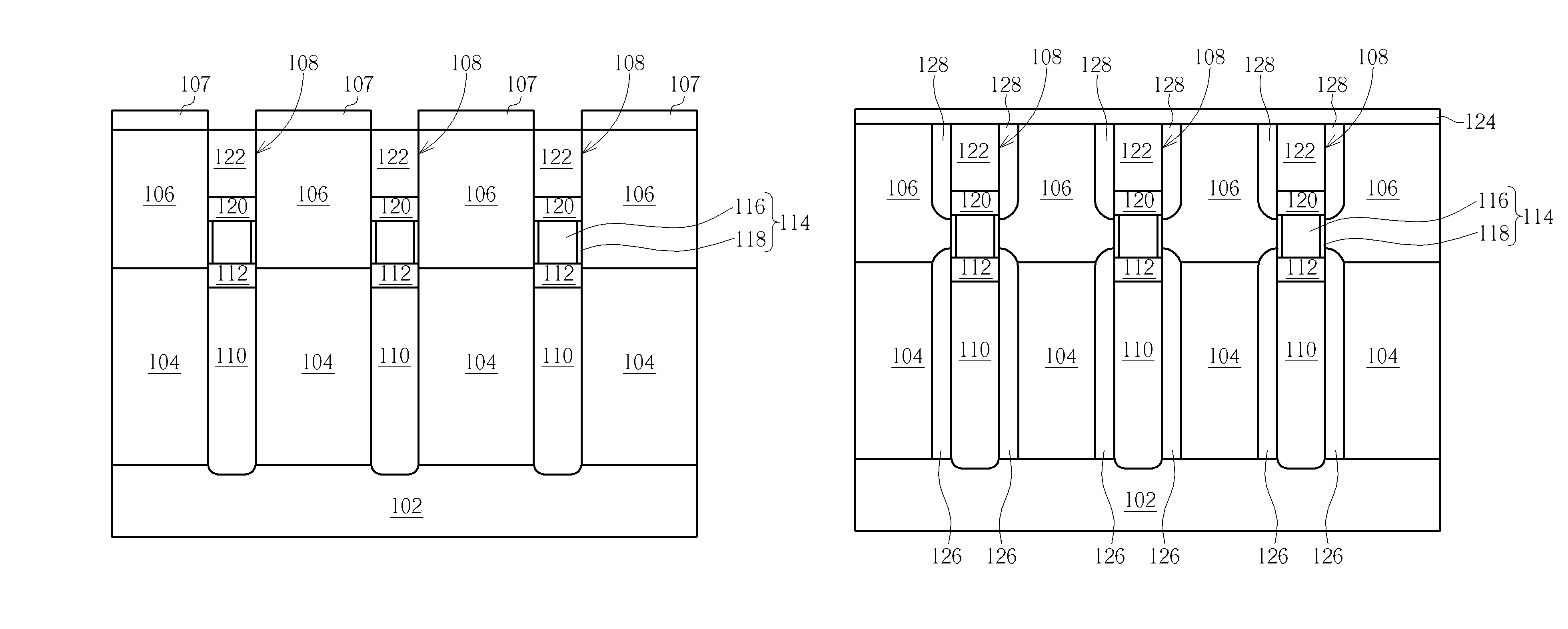
[0014]Please refer to FIGS. 7-12, which are schematic views illustrating the manufacturing method of a power transistor device in accordance with the first embodiment of present invention. First, as shown in FIG. 7, a substrate 102 of a first conductive type having an active device region and a peripheral region is provided. The following description will take the power transistor device in the active device region as an example to be manufactured. An epitaxial process is then carried out to form an epitaxial layer 104 having a second conductive type different from the first conductive type on the substrate 102. Then, a first ion implantation process of the second conductive type and a first thermal drive-in process are performed to form a doped base region 106 of the second conductive type in the epitaxial layer 104. Then, a pad layer 107 is formed on the doped base region 106. The pad layer 107 may be made of materials, such as silicon dioxide (SiO2), silicon nitride (Si3N4), or a...


PUM


Abstract

The present invention provides a power transistor device including a substrate, an epitaxial layer, a dopant source layer, a doped drain region, a first insulating layer, a gate structure, a second insulating layer, a doped source region, and a metal layer. The substrate, the doped drain region, and the doped source region have a first conductive type, while the epitaxial layer has a second conductive type. The epitaxial layer is formed on the substrate and has at least one through hole through the epitaxial layer. The first insulating layer, the gate structure, and the second insulating layer are formed sequentially on the substrate in the through hole. The doped drain region and doped source region are formed in the epitaxial layer at one side of the through hole. The metal layer is formed on the epitaxial layer and extends into the through hole to contact the doped source region.

Description

BACKGROUND OF THE INVENTION[0001]1. Field of the Invention[0002]The present invention relates generally to a power transistor device and a manufacturing method thereof, more particularly, to a trench type power transistor device with a super junction and a manufacturing method thereof.[0003]2. Description of the Prior Art[0004]In power transistor devices, the ON resistance (RDS(on)) between the drain and the source is proportional to the power consumption of the device, so an effective way to reduce the power consumption of the power transistor device is to lower the RDS(on). In power transistor devices, the resistance provided by the epitaxial layer used for withstanding high voltage is the main contribution to the RDS(on). Although increasing the doping concentration of the conductive material in the epitaxial layer can reduce the resistance, the breakdown voltage of the epitaxial layer will also be lowered, thereby degrading the capacity of the power transistor device to withstan...

Claims


Application Information

Patent Timeline
Patent Type & Authority Patents(United States)
IPC IPC(8): H01L21/336H01L21/22H01L21/38
CPCH01L21/2255H01L29/7827H01L29/4236H01L29/66734H01L29/7813H01L29/0634H01L29/66727H01L29/41766H01L29/41775H01L29/0869H01L29/0653H01L29/0886
Inventor LIN, YUNG-FAHSU, SHOU-YIWU, MENG-WEICHEN, MAIN-GWOCHANG, CHIA-HAOCHEN, CHIA-WEI
Owner ANPEC ELECTRONICS CORPORATION
Why Eureka
Try Eureka