Semiconductor device with improved ESD protection

a technology of shielding and semiconductor devices, applied in the direction of semiconductor devices, semiconductor/solid-state device details, diodes, etc., can solve the problems of parasitic resistance high voltage overshoots between the electrodes of the diode, and the diode is not suitable for fast switching characteristics, so as to reduce the resistance between them, reduce the electrical resistance of the series connection of the diode, and reduce the resistance of the diod

Active Publication Date: 2013-09-24
NXP BV
View PDF8 Cites 8 Cited by
  • Summary
  • Abstract
  • Description
  • Claims
  • Application Information

AI Technical Summary

Benefits of technology

[0008]The semiconductor device of the first aspect of the present invention provides a protection against ESD-related damage with a structure that allows obtaining fast switching characteristics in a combination with a high reverse breakdown voltage.
[0019]In one embodiment, at most two diodes are arranged in a respective substrate island. In any case, where two diodes are arranged in one substrate island, they are preferably provided in a back-to-back configuration of the series connection of diodes. This configuration can be achieved by laterally arranging substrate regions of the second conductivity type in a respective substrate island of the first conductivity type, with a lateral distance from each other. As an example, where the side length of a diode is 200 Micrometer, a suitable distance between two neighboring diodes is approximately 100 Micrometer. This arrangement of two back-to-back diodes in one substrate island helps reducing the resistance between them.
[0020]A further reduction of the electrical resistance of the series connection of diodes is achieved in an embodiment, in which the substrate has a thickness of less than less than 50 Micrometer. In one example with a particularly low resistance of the series connection of diodes, the thickness of the semiconductor substrate is even only 20 Micrometer. As explained before, reducing the electrical resistance between the individual diodes further enhances the switching speed. The rise time of less than 1 Nanosecond can be achieved during the initial high-current peak in test configurations such as the “gun test model” of the norm IEC 6100-4-2. However, special attention is required for processing such semiconductor devices with thin semiconductor substrates.
[0022]The semiconductor device is suitably provided with other circuit elements such as capacitors or inductors. Capacitors can be used for decoupling an integrated circuit connected with the semiconductor device either on the same semiconductor substrate or on a different semiconductor substrate. Inductors can be used to force an ESD current through the series connection of diodes and avoid a current flow through a connected integrated circuit.
[0037]This processing keeps the semiconductor stable during and after the thinning step.

Problems solved by technology

While a high reverse trigger voltage alone, such as for instance 60 Volt, can be reached in prior-art semiconductor devices with single Zener or avalanche diodes, such diodes are not suitable for achieving fast switching characteristics.
As a consequence, during an initial short high-current peak of an ESD event, high voltage overshoots would be observed between the electrodes of this parasitic resistance, when using such a high-voltage Zener or avalanche diode.

Method used


Image

  • Semiconductor device with improved ESD protection
  • Semiconductor device with improved ESD protection
  • Semiconductor device with improved ESD protection

Examples


Embodiment Construction

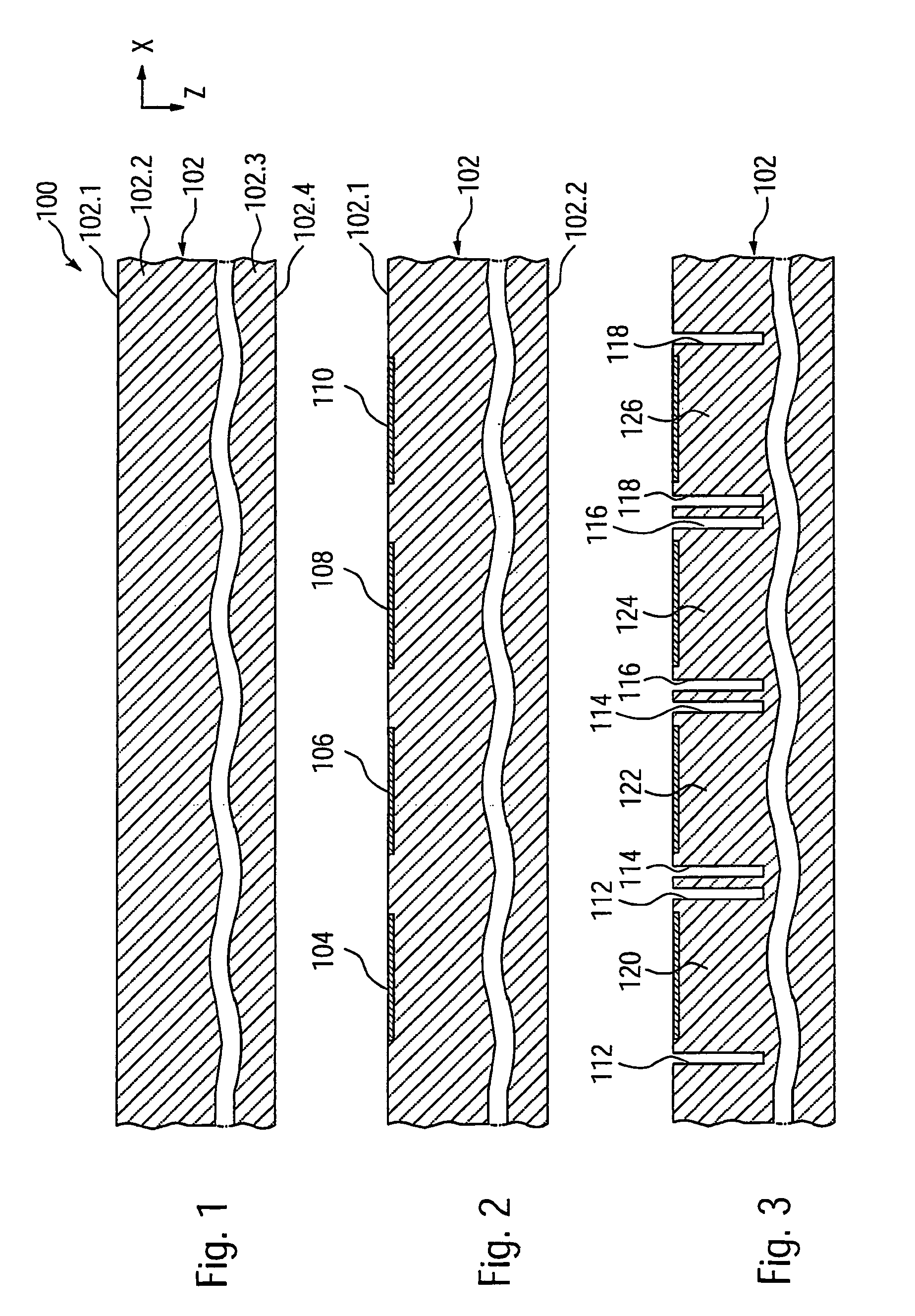
[0048]FIGS. 1 to 10 show schematic cross sectional views of a semiconductor device according to a first embodiment during different stages of its fabrication.

[0049]FIG. 1 shows a semiconductor device 100 at an initial stage of its fabrication. At this point, a semiconductor substrate 102 is provided. The semiconductor substrate 102 is only shown in a lateral section relevant for describing the ESD protection structure. Also, to make features fabricated during subsequent processing steps on a first substrate side 102.1 better visible, only a top substrate region 102.2 extending near the first substrate side 102.2 and a bottom substrate region 102.3 extending near a second substrate side 102.4 are shown in FIG. 1 and the following Figures. In the following description, use of the word “top” and “bottom” is made only with respect to a representation of the semiconductor device 100 in the enclosed drawings on paper or on a screen, and does not imply any restriction on the usage or arran...


PUM


Abstract

The present invention relates to a semiconductor device, comprising a semiconductor substrate (102) with a thickness of less than 100 micrometer and with a first substrate side and an opposite second substrate side. A plurality of at least four monolithically integrated Zener or avalanche diodes (164,166,168,170) with a reverse breakdown voltage of less than 20 V are defined in the semiconductor substrate and connected with each other in a series connection. The diodes are defined in a plurality of mutually isolated substrate islands (120,122,124,126) in the semiconductor substrate, at least one diode per substrate island. The substrate islands are laterally surrounded by through-substrate isolations extending from the first to the second substrate side and comprising a filling (128) that electrically isolates a respective substrate island from a respective laterally surrounding area of the semiconductor substrate.

Description

FIELD OF THE INVENTION[0001]The present invention relates to a semiconductor device, a semiconductor assembly comprising a first and a second semiconductor device, and to a method for fabricating a semiconductor device. The invention relates to the field of protection of a semiconductor device against electrostatic discharge (ESD). Without restricting the applicability of the invention, an example of an application field of the invention is a semiconductor device for automotive applications.BACKGROUND OF THE INVENTION[0002]Many semiconductor devices comprising integrated circuits have an ESD protection structure monolithically integrated within the semiconductor substrate. For instance, in the field of automotive applications, transceiver ICs for Control Area Network (CAN) communication may comprise monolithically integrated ESD protection structures.[0003]Known ESD protection structures comprise monolithically integrated back-to-back Zener or avalanche diodes. For instance, U.S. Pa...

Claims


Application Information

Patent Timeline
Patent Type & Authority Patents(United States)
IPC IPC(8): H01L29/866H01L21/762
CPCH01L23/60H01L27/0255H01L27/0814H01L23/481H01L25/167H01L2924/3011H01L2224/02372H01L2224/131H01L2224/0401H01L2224/05548H01L2224/13024H01L2924/00014
Inventor YANNOU, JEAN-MARCVAN ZWOL, JOHANNESSAVIN, EMMANUEL
Owner NXP BV
Why Eureka
Try Eureka